


 +86-731-89578196
 [email protected]

- Home
- Our Company
-
Products
Sputtering Targets

- Industries
- Blog
- FAQ
- Contact Us


Choosing the Right Silicon Sputtering Target: Grades, Specs & Buying Tips
Introduction — Why Silicon Sputtering Targets Matter Today
Silicon sputtering targets are widely used to create thin films for semiconductors, displays, solar cells, and optical devices. Because these films must be clean and consistent, the quality of the silicon target directly affects coating performance and production yield.
In sputtering, silicon atoms are released from the target and form a thin layer on the substrate. If the target has low purity, poor density, or uneven structure, the resulting film can develop defects or unstable electrical properties.
Choosing the right silicon sputtering target—correct grade, purity level, and reliable supplier—is essential for a stable process and high-quality films. This guide explains the key grades, important specifications, and practical tips to help you select the best silicon target for your application.
Understanding Silicon Sputtering Targets — Basics Engineers Should Know
What Is a Silicon Sputtering Target?
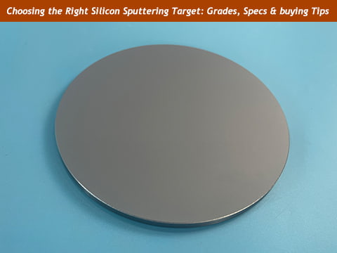
A silicon sputtering target is a solid block of high-purity silicon used in PVD sputtering systems to deposit thin silicon films. When ions strike the target surface, silicon atoms are ejected and form a uniform coating on the substrate. These films are used in semiconductor devices, TFT backplanes, optical coatings, and other electronic components.
Silicon targets come in several forms depending on equipment and application needs—such as planar targets, rotary targets, single-crystal, poly-crystal, and doped versions. Each has different advantages for film quality, deposition rate, and electrical performance.
Production Routes for Silicon Sputtering Targets
Silicon targets can be produced in different ways, and the chosen route affects purity, grain structure, and sputtering stability.
Zone Refining (for ultra-high-purity silicon)
Zone refining is a process where a narrow molten zone moves along a silicon rod to remove impurities. It is commonly used for 5N–9N single-crystal silicon, ideal for semiconductor and precision optical coatings. This method creates extremely pure and uniform material.
Powder Metallurgy (for poly-crystalline silicon)
Poly-crystal silicon targets are often made using powder metallurgy. Fine silicon powders are pressed, sintered, and then densified. This produces a stable structure suitable for large-area coatings, display manufacturing, and general PVD applications.
CNC Machining & Surface Grinding
Regardless of the production route, all silicon targets undergo precision machining to achieve the required diameter, thickness, and mounting features. Final surface grinding ensures excellent flatness and uniform sputtering behavior.
Why Production Method Matters
Different production methods lead to different target properties:
- Purity: Higher purity reduces defects and contamination.
- Density: Dense targets sputter more evenly and last longer.
- Grain Structure: Crystal type affects sputtering rate and film consistency.
Understanding these basics helps engineers and buyers choose the right silicon target for their specific coating line and performance requirements.
Key Grades of Silicon Sputtering Targets
Silicon sputtering targets come in several grades, each designed for different film requirements and equipment setups. Understanding the differences helps you select the right material for your thin-film process.
Single-Crystal Silicon Targets
Single-crystal silicon (c-Si) targets are made using high-purity silicon refined through zone refining and crystal-pulling methods such as CZ or FZ. These targets have a uniform crystal structure with no grain boundaries, which provides:
- Very stable sputtering behavior
- Low particle generation
- Highly consistent electrical and optical film properties
They are commonly used in semiconductors, MEMS devices, advanced optical coatings, and other applications that require the highest purity and film uniformity.
Typical purity: 5N–9N (99.999%–99.9999999%)
Polycrystalline Silicon Targets
Polycrystalline silicon (poly-Si) targets consist of many small grains instead of one continuous crystal. They are usually produced by powder metallurgy, which offers excellent control over density and shape.
Poly-Si targets are more cost-effective and work well for:
- TFT-LCD backplanes
- Photovoltaic and solar cell coatings
- Large-area PVD coating lines
- General electronic thin films
Typical purity: 4N–6N depending on the application.
They provide good sputtering stability while keeping production costs reasonable.
Doped Silicon Targets (Boron, Phosphorus, Arsenic)
For applications that require controlled electrical properties, silicon targets can be doped with small amounts of elements such as boron (p-type) or phosphorus/arsenic (n-type).
Doped silicon sputtering targets are widely used in:
- TFT-LCD and OLED display backplanes
- Semiconductor device fabrication
- Solar panels requiring specific resistivity levels
Doping helps engineers control film resistivity, improve conductivity, and fine-tune device performance.
How to Choose Between These Grades
- Choose single-crystal when purity, film uniformity, and electrical stability are the highest priority.
- Choose poly-Si when you need a cost-effective, stable material for large-area coating.
- Choose doped silicon when your process requires specific electrical characteristics.
Understanding these grades sets the foundation for selecting the most suitable silicon sputtering target for your equipment and product requirements.
Comparison with Other Sputtering Targets
Silicon sputtering targets are valued for their tunable electrical properties, stable purity, and wide use in semiconductor and display manufacturing. However, depending on the type of film required, other sputtering materials may offer advantages in conductivity, adhesion, or optical performance.
– ITO (Indium Tin Oxide)
ITO is the industry standard for transparent conductive films, making it essential for touchscreens and display panels.
While silicon cannot provide the same level of transparency or conductivity, ITO is more expensive and depends heavily on indium supply, making it less suitable for applications where cost stability is important.
– Aluminum (Al)
Aluminum is commonly chosen for metal layers because it is affordable, deposits quickly, and offers strong electrical conductivity.
Unlike silicon, aluminum cannot act as a semiconductor or dielectric layer, so it is limited to conductive and reflective applications.
– Titanium (Ti)
Titanium is preferred when a coating requires strong adhesion or a durable barrier layer. It bonds well to many substrates and is widely used in multilayer film stacks.
However, titanium does not provide the electrical or optical functions that silicon can, so it typically serves as a supporting layer rather than the main active material.
– Silicon Oxide (SiO₂) and Other Oxides
Oxide targets such as SiO₂, Al₂O₃, and TiO₂ are often used for insulating, optical, or hard-coating layers.
These materials offer higher transparency and stronger dielectric properties compared with pure silicon, but they lack the controllable resistivity and semiconductor behavior that make silicon useful in electronics.
– Germanium (Ge) and Other Semiconductor Materials
Germanium and compound semiconductors like GaAs are used when higher carrier mobility or infrared performance is required.
Although these materials outperform silicon in certain specialized devices, they come with higher cost and more complex processing requirements.
Each sputtering material has a unique role: ITO for transparent conductors, aluminum for metal layers, titanium for adhesion, oxides for insulation, and Ge/GaAs for niche semiconductor needs. Silicon remains the most versatile option when a balance of electrical control, stability, and cost efficiency is needed.
Conclusion
Silicon sputtering targets are a key part of many modern coating processes, especially in semiconductors, displays, and solar technologies. But not all targets are created equal. Choosing the right one means understanding your application, knowing what grade and purity level you need, and making sure the target fits your equipment and process conditions.
Whether you're working with doped silicon for display backplanes or high-purity single-crystal silicon for advanced chips, the quality of the target affects every step of production—from sputtering stability to film performance.
That's why it's important to work with a supplier who not only provides high-quality materials, but also understands the technical requirements behind them. At AEM Deposition, we offer silicon sputtering targets with customizable specifications, strict purity control, and global support—so you can focus on results, not guesswork.