


 +86-731-89578196
 [email protected]

- Home
- Our Company
-
Products
Sputtering Targets

- Industries
- Blog
- FAQ
- Contact Us


What Is Germanium Used For? Thin-Film Applications Explained
Introduction
Germanium is a special material used in many high-tech industries. While it’s not as famous as silicon, germanium has unique properties that make it valuable for electronics, solar panels, infrared cameras, and other advanced devices.
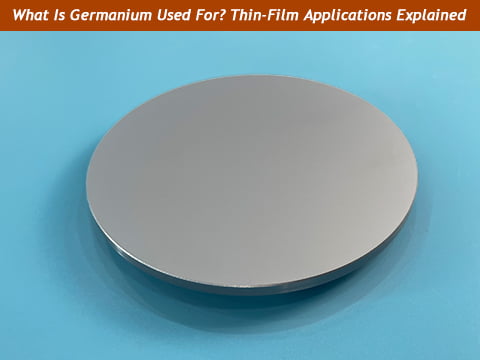
In thin-film manufacturing, germanium is often turned into a sputtering target or evaporation material. These are used to coat other materials with a very thin, even layer of germanium. This process is common in making semiconductors, optical lenses, and memory devices.
To get the best performance, these coatings need very pure germanium—usually 99.999% purity or higher. That’s why the quality of the germanium target is so important.
At AEM Deposition, we supply high-purity germanium sputtering targets made with advanced techniques like zone refining. This helps remove tiny impurities and ensures the germanium works well in sensitive applications.
What Is Germanium? Key Properties & Forms
Germanium is a gray-white, shiny metal-like element that belongs to the same chemical group as silicon. It is known for being a semiconductor, which means it can conduct electricity under certain conditions—an important feature in electronics and thin-film technologies.
Basic Facts About Germanium
- Symbol: Ge
- Atomic Number: 32
- Melting Point: About 938°C
- Density: 5.32 g/cm³
- Crystal Structure: Diamond cubic (like silicon)
Germanium is found in small amounts in the earth’s crust and is usually extracted from zinc ores or coal byproducts. Because it's naturally rare, most germanium used in thin films must be carefully purified to meet high standards.
Special Properties That Make Germanium Valuable
-
Semiconductor Behavior
Germanium is sensitive to electric signals and is used in transistors, diodes, and solar cells. It offers fast electron mobility, which helps improve the performance of electronic devices. -
Infrared Transparency
Germanium can transmit infrared (IR) light, making it useful in night vision devices, thermal cameras, and IR optics. -
High Refractive Index
It bends light strongly, which is useful in optical lenses and coatings. -
Stable & Pure in Thin Films
When made into sputtering targets or evaporation materials, germanium forms uniform, stable coatings for various advanced applications.
Germanium in Thin-Film Deposition Technologies
Germanium plays a vital role in the fabrication of advanced thin-film materials used in electronics, optoelectronics, and infrared optics. It is most commonly applied via Physical Vapor Deposition (PVD) techniques, such as sputtering and thermal evaporation, where its purity, stability, and film-forming properties are critical to performance.
Sputtering Deposition
In magnetron sputtering, high-purity germanium sputtering targets are installed within a vacuum chamber. An inert gas (typically argon) is introduced, and a strong electric field is applied, generating a plasma. The resulting ion bombardment dislodges Ge atoms from the target, which then condense onto the substrate to form a uniform thin film.
This technique is widely used for:
- Semiconductor device metallization
- IR-reflective and anti-reflective coatings
- Memory storage layers (e.g., in Ge–Sb–Te alloys)
Sputtering offers excellent film uniformity, adhesion, and control over thickness—key factors for high-precision applications.
Thermal Evaporation
Germanium can also be deposited by thermal or electron-beam (e-beam) evaporation, in which the material is heated under high vacuum until it vaporizes. The vapor then condenses on the target surface, creating a dense, adherent film.
Evaporation is preferred when:
- Ultra-high purity is required
- Substrate temperatures must be minimized
- Simple planar coating geometry is sufficient
It is particularly common in IR optics, photovoltaic cells, and research-scale semiconductor fabrication.
Importance of Purity in Germanium Thin Films
Thin-film performance is highly sensitive to contamination. Trace elements or oxygen levels can alter the electrical and optical behavior of the final coating. For this reason, 5N (99.999%) or higher purity is typically required, especially in semiconductor and photonic applications.
At AEM Deposition, we supply zone-refined and vacuum-processed germanium materials tailored for demanding PVD applications, ensuring stable deposition rates, low contamination, and excellent thin-film integrity.
Zone Refining: How High-Purity Germanium Targets Are Made
To meet the ultra-high purity demands of semiconductor and optical thin-film applications, zone refining is one of the most effective methods for producing 5N–6N purity germanium. This process is especially important when conventional vacuum melting cannot achieve the required level of purity or crystal uniformity.
What Is Zone Refining?
Zone refining is a precision purification technique used to remove metallic and non-metallic impurities from semiconductor-grade materials such as germanium (Ge). Unlike full-melt processes, zone refining involves localized melting of the material along a solid rod.
The basic principle is based on the fact that impurities distribute unevenly between solid and liquid phases. As a narrow molten zone travels slowly along the germanium rod, impurities are concentrated and carried toward one end of the material. This process can be repeated multiple times to push contaminants into a small, removable section.
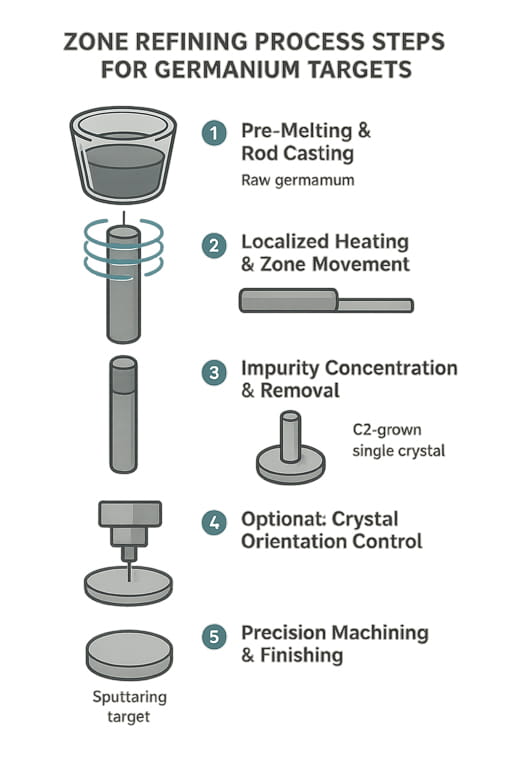
Zone Refining Process Steps for Germanium Targets
-
Pre-Melting & Rod Casting
Raw germanium is initially melted in a high-purity quartz crucible and cast into a cylindrical rod, which serves as the base material for zone refining. -
Localized Heating & Zone Movement
A high-frequency induction coil creates a narrow molten zone that slowly moves along the rod under an inert atmosphere. This causes impurities to migrate with the molten front. -
Impurity Concentration & Removal
After several passes, the impurities accumulate at one end of the rod. This section is cut off and discarded, leaving behind a highly purified germanium body. -
Optional: Crystal Orientation Control
In some cases, single-crystal structures can be grown from the refined germanium using Czochralski (CZ) methods for applications that require precise crystallographic orientation. -
Precision Machining & Finishing
The purified germanium is then sliced, ground, and CNC-machined into sputtering targets with tight tolerances and uniform thickness, ready for vacuum deposition.
Thin-Film Applications of Germanium
Germanium's role in thin-film deposition spans multiple high-tech sectors, including semiconductors, optoelectronics, photovoltaics, and data storage. Its exceptional properties—such as infrared transparency, high refractive index, and excellent carrier mobility—make it an essential material in the design and manufacturing of next-generation devices.
Below is a comprehensive overview of the major application areas where germanium thin films, prepared via sputtering or evaporation, are used.
1. Infrared Optics and Thermal Imaging Systems

Germanium is one of the most widely used materials in infrared (IR) optical systems, thanks to its transparency in the 2–14 μm wavelength range. When deposited as a thin film, it serves as a high-index layer in infrared coatings, enabling precise control over light reflection, transmission, and absorption.
Thin-film IR applications include:
- Germanium-coated IR lenses and windows for night vision goggles, thermal cameras, and surveillance systems
- Beam splitters and anti-reflective coatings for multispectral imaging systems
- Protective and enhancing coatings for laser optics in aerospace and defense
Due to its high refractive index (~4.0 in the IR range), germanium is often paired with materials like ZnS, ZnSe, or YF₃ in multilayer coatings. Purity and thickness control are crucial to ensure minimal optical losses and long-term environmental stability.
2. Semiconductor Devices and High-Frequency Electronics

While silicon dominates most commercial semiconductor applications, germanium offers higher electron and hole mobility, making it a top choice for high-speed and low-power electronics. Thin germanium films are increasingly used in:
- P-N junction diodes and power rectifiers requiring fast switching speed
- Heterojunction bipolar transistors (HBTs) for RF and microwave circuits
- Germanium-on-Insulator (GeOI) and Germanium-on-Silicon (Ge/Si) structures in CMOS scaling
- Photodetectors and modulators in silicon photonics
As demand grows for next-generation logic and optoelectronic integration, Ge thin films enable enhanced channel mobility and compatibility with existing silicon platforms.
3. Photovoltaic Devices and Space-Grade Solar Panels

In multi-junction solar cells, germanium functions as both a bottom cell and a lattice-matched substrate for the growth of III-V semiconductor layers such as GaAs, InGaP, and InGaAs. These thin-film devices are critical in environments where efficiency, weight, and durability are paramount—particularly in space applications.
Key roles of germanium thin films in solar technologies:
- Substrate layer for epitaxial growth in triple-junction solar cells
- Back-surface field (BSF) or reflective layers to improve photon capture
- Thermally stable platform that withstands extreme environments in satellites and aerospace
AEM Deposition supplies zone-refined Ge targets ideal for vacuum deposition in cleanroom and aerospace-grade production.
4. Phase-Change Memory and Optical Data Storage

Germanium is a critical component in Ge–Sb–Te (GST) phase-change materials, widely used in non-volatile memory (PCM) and rewritable optical discs. In thin-film form, GST can rapidly switch between amorphous and crystalline states under controlled heating, enabling fast and reliable data storage.
Applications include:
- Thin-film phase-change memory (PCM) used in embedded systems and mobile devices
- Rewritable DVDs and Blu-ray discs
- Emerging use in neuromorphic computing and optical logic gates
In these applications, precise deposition and composition control of germanium-based thin films are essential to achieving uniform switching thresholds, long cycling life, and data retention performance.
5. Research & Development of Quantum and Photonic Devices

With the rapid evolution of quantum computing and integrated photonics, germanium is now being investigated and used in:
- Superconducting junctions and qubits
- Waveguides and photonic crystals for on-chip optics
- High-mobility p-type channels in advanced transistors
Thin-film germanium enables tunable bandgaps and efficient light absorption/emission, making it a strong candidate for photonic integration on silicon chips.
Conclusion
Germanium is a powerful and versatile material in the world of thin-film technology, with applications ranging from infrared optics and semiconductors to photovoltaics and data storage. Whether you're working on advanced solar cells, IR coatings, or phase-change memory, the quality of your thin-film coating starts with the right target.
At AEM Deposition, we specialize in supplying high-purity germanium sputtering targets—customized, bonded, and tested to meet your exact deposition needs. With zone refining capabilities, tight tolerance machining, and comprehensive QA procedures, we support engineers and manufacturers across industries in achieving consistent, high-performance thin films.