 +86-731-89578196
 [email protected]
- Home
- Our Company
-
Products
Sputtering Targets
- Industries
- Blog
- FAQ
- Contact Us
Glass Substrates and Wafers for MEMS Applications
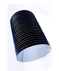
Microelectromechanical (MEMS) and microsystem developers worldwide trust AEM Deposition to provide high-performance MEMS glass wafers and substrates for their prototype and production processing.
Sizes of MEMS Glass Wafers
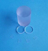
AEM Deposition offers MEMS glass wafers and polished glass substrates, both structured and blanks, in standard and non-standard sizes through 8” (200 mm). Our existing capability support the production of 12” (300 mm) MEMS glass wafers.
Quality and Precision
AEM Deposition glass wafers set the standard for quality and precision, allowing you to focus on your process and design's critical details, rather than the quality and consistency of supplier parts.
Applications of AEM Deposition MEMS Glass Wafers
AEM Deposition glass wafers and substrates are used in a wide range of MEMS applications, including pressure sensors, inertial measurement units, DNA analysis, and implantable sensors.
Properties of AEM Deposition MEMS Glass Wafers
Technical Assistance
AEM Deposition's experienced staff is knowledgeable regarding MEMS processes and applications and is qualified to assist you in solving your most complex MEMS development challenges. Our technical team can help you select the glass micro-fabrication processes that are best suited for your application.


