


 +86-731-89578196
 [email protected]

- Home
- Our Company
-
Products
Sputtering Targets

- Industries
- Blog
- FAQ
- Contact Us


Principle of Chemical Vapor Deposition (CVD)
views, Updated: 2025-04-09
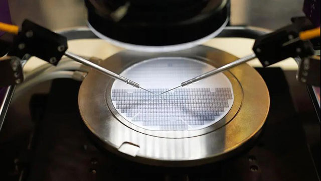
Chemical vapor deposition (CVD) is a well-known technology in the field of nanomanufacturing. It is often used in large-scale integrated circuits, insulating materials, magnetic materials, optoelectronic materials.
Chemical vapor deposition (CVD) and Physical vapor deposition(PVD) are two different processes used to deposit thin films of material onto a substrate. Both CVD and PVD are widely used in the semiconductor industry and other fields to produce thin films for a variety of applications.
Chemical vapor deposition (CVD) and Physical vapor deposition(PVD) are two different processes used to deposit thin films of material onto a substrate. Both CVD and PVD are widely used in the semiconductor industry and other fields to produce thin films for a variety of applications.
Chemical vapor deposition (CVD) can deposit evaporated reactants on the surface to form thin-films. For example, graphene is the most widely recognized product of CVD. So, what is the principle of CVD?
Principle of Chemical Vapor Deposition (CVD)
CVD has been studied since the end of the 19th century. It is mainly used in the synthesis and preparation of important materials. If we want to know how CVD makes a specific film, we must first understand its principle.
CVD belongs to the "bottom-up" technology. Its principle is to introduce the vapor of gaseous or liquid reactant containing film elements and other gases needed to react into the reaction chamber. By increasing the temperature, plasma action, light radiation, or other forms of energy, CVD can produce chemical reactions on the substrate surface and generate new solid substances to be deposited on the surface.
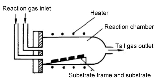
Schematic diagram of CVD method
CVD consists of four main stages:
① The reaction gas diffuses to the surface of the material.
② The reaction gas is adsorbed on the surface of the material.
③ Chemical reaction occurs on the surface of the material.
④ The gaseous by-products are separated from the material surface.
Because of the molecular level nucleation or growth, CVD is more suitable for forming dense and uniform films on the irregular substrate surface. CVD deposition speed is fast, and film quality is stable. Some notable films also have excellent optical, thermal, and electrical properties, making it easy to achieve mass production.
The deposition temperature of CVD is usually very high, between 900 ℃ ~ 2000 ℃, it is easy to cause the deformation of parts and the change of structure so as to reduce the mechanical properties of the body material and weaken the binding force between the body material and the coating, which limits the selection of substrate, the deposition layer or the quality of the workpiece. Therefore, low temperature and high vacuum are the main development direction of CVD.
Our company AEM Deposition as one of professional manufacturer of evaporation materials and sputtering targets, We offer a full range of high purity elemental and composite evaporation materials in various purities and dimensions to meet any customer needs. If you have any questions or raw material inquiry, please feel free to contact us anytime.
Our company AEM Deposition as one of professional manufacturer of evaporation materials and sputtering targets, We offer a full range of high purity elemental and composite evaporation materials in various purities and dimensions to meet any customer needs. If you have any questions or raw material inquiry, please feel free to contact us anytime.
LATEST NEWS