


 +86-731-89578196
 [email protected]

- Home
- Our Company
-
Products
Sputtering Targets

- Industries
- Blog
- FAQ
- Contact Us


Your Essential Guide to Semiconductor Materials: From Silicon to Gallium and Germanium
Introduction: The Silent Power Behind Modern Electronics
Semiconductor materials are at the heart of nearly every electronic device we use today. From smartphones and laptops to electric vehicles and solar panels, these materials make modern technology possible. While we rarely see them, semiconductors quietly power the digital world around us.
They’re not just materials—they’re enablers. Without semiconductors, computers wouldn’t process information, phones wouldn’t connect, and renewable energy systems wouldn’t work as efficiently. Simply put, semiconductors are the building blocks of the connected age.
As technology becomes faster, smaller, and smarter, the role of semiconductor materials becomes even more important. Governments, tech companies, and research institutions across the globe are investing heavily in these materials to drive innovation and meet the demands of future technologies.
What Are Semiconductor Materials?
Semiconductor materials are special substances that can carry electricity—but only under certain conditions. They don’t conduct electricity as easily as metals like copper, but they’re not complete insulators like plastic either. This in-between behavior is what makes them so valuable in electronics.
What really sets semiconductors apart is their ability to control the flow of electricity. Depending on how they’re treated or designed, they can either block or allow current to pass through. That makes them perfect for building things like microchips, transistors, and solar cells.
The most well-known semiconductor is silicon, mainly because it’s easy to work with and found in abundance. But there are others too—germanium and gallium-based materials, for example, are used in specific applications like high-speed electronics and LED lights.
Key Electrical Properties That Make a Material “Semiconducting”
So what makes these materials so useful in electronics? Here are a few key features:
- Controlled conductivity: Semiconductor materials don’t always conduct electricity. They can be turned "on" or "off" by adding energy—like heat, light, or voltage. That’s why they’re great for making switches and logic gates in electronic circuits.
- Doping: This is a process where small amounts of other elements are added to the material to improve its electrical performance. For example, adding phosphorus or boron to silicon helps fine-tune how it handles electricity.
- Adjustable behavior: Semiconductors can be designed to behave differently depending on the device's needs. Some are made for speed, others for handling high power, and some for use in extreme conditions like space or heat.
- Form flexibility: These materials come in different forms—wafers, powders, ingots, and even liquid metals—to suit various manufacturing processes.
Thanks to these properties, semiconductor materials can be shaped into just about anything: the processor in your computer, the screen on your phone, or the sensor in your car. They’re adaptable, reliable, and absolutely essential in our technology-driven world.
Most Commonly Used Semiconductor Materials
Semiconductors come in many types, but a few materials are used far more often than others. Each has its own strengths and is chosen based on what the device or application needs—whether that’s speed, power, precision, or durability.
Let’s take a closer look at the most common semiconductor materials used today and why they matter.
Silicon (Si)
Silicon is by far the most widely used semiconductor material—and for good reason. It’s abundant, affordable, and works well in most electronic devices. Silicon is the material behind almost every computer chip and smartphone processor on the planet.
What makes silicon so valuable is how easily it can be modified to control electricity. It also forms a strong, stable crystal structure, which is ideal for making wafers, the thin slices used to build circuits and chips.
Silicon isn’t just used in solid wafers—it’s also processed into thin-film layers for things like solar panels and display technology. In those applications, it’s often used in the form of sputtering targets made from pure silicon, or from compounds like SiO (silicon monoxide) and SiO₂ (silicon dioxide), depending on the coating requirements.
Germanium (Ge)
Germanium was actually the first material used in early transistors before silicon took over. Today, it’s still important in areas where speed and precision are needed—such as in infrared optics, high-frequency circuits, and fiber-optic communication.
Germanium stands out because it allows electrons to move more easily compared to silicon, which makes it great for high-speed devices. It also has excellent sensitivity to light, making it a popular choice for photodetectors and sensors.
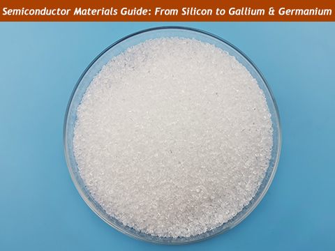
Depending on the application, germanium can be supplied in different forms like powders, ingots, crystals, or granules. This flexibility makes it useful for both research and commercial production.
Gallium (Ga)
Gallium isn’t used on its own very often, but when combined with other elements—like arsenic or nitrogen—it forms powerful compound semiconductors such as gallium arsenide (GaAs) and gallium nitride (GaN).
These materials are key in advanced technologies where speed, power, and high efficiency are critical. For example, GaAs is used in satellite communication and mobile phones, while GaN is common in LED lighting and high-voltage power electronics.
Gallium is available in various forms—granules, shots, liquids—depending on how it's going to be used in manufacturing or research. It plays a vital role in devices that need to handle high temperatures or operate at very high frequencies.
Other Semiconductor Materials
While silicon, germanium, and gallium are the most common, there are other materials used in special applications:
- Silicon Carbide (SiC): Great for high-power electronics and electric vehicles.
- Indium Phosphide (InP): Used in high-speed fiber-optic systems.
- Organic semiconductors: Found in flexible electronics and OLED displays.
Each of these has a niche where it performs better than traditional materials, especially as devices get more advanced.
Quick Comparison
|
Material |
Best Known For |
Common Applications |
|---|---|---|
|
Silicon |
Versatility and cost-efficiency |
Processors, solar cells, sensors |
|
Germanium |
High-speed performance and infrared use |
Optics, detectors, high-frequency circuits |
|
Gallium |
High efficiency and frequency |
LEDs, RF amplifiers, power devices |
|
SiO / SiO₂ |
Insulation and coating |
Displays, solar tech, microelectronics |
In short, these materials are chosen not just for how they conduct electricity, but also for how they fit into a product’s design and function. Whether it’s improving speed, shrinking size, or saving energy—each semiconductor material has a role to play in powering the technology we depend on every day.
Understanding Semiconductor Wafers
Semiconductor wafers are the thin, circular slices of material that serve as the foundation for building electronic circuits. They’re where all the magic of chips, sensors, and microprocessors begins. If semiconductor materials are the ingredients, wafers are the platform where everything comes together.
These wafers are made by cutting slices from a solid crystal—called an ingot—which has been carefully grown to have a pure and uniform atomic structure. The wafer is then polished to a mirror-like finish and used as a base for manufacturing tiny electronic components through a process known as photolithography.
Why Wafers Matter
Without wafers, you couldn’t create the complex layers of circuitry that power devices. They offer a stable, flat surface where manufacturers can build incredibly small structures—thousands of times thinner than a human hair.
Think of wafers like a blank sheet of paper. On this surface, patterns are drawn, etched, and layered using advanced techniques to form millions (or even billions) of transistors, memory cells, and other essential parts of electronic devices.
Silicon Wafers: The Industry Standard
Most of the wafers used in electronics today are made from silicon. Silicon wafers come in different sizes, typically ranging from 100 mm to 300 mm in diameter. Larger wafers allow for more chips to be made from a single slice, which reduces manufacturing costs and improves efficiency.
Silicon wafers are popular because they offer a good balance between performance, availability, and cost. They’re used in everything from everyday smartphones and laptops to high-performance servers and smart home devices.
Germanium Wafers: Precision in Optics and Speed
While not as common as silicon, germanium wafers play a key role in specialized applications. They are valued for their high electron mobility and optical clarity, which makes them ideal for:
- Infrared optics
- Photodetectors
- High-speed integrated circuits
Germanium wafers are often used in research labs, aerospace technology, and telecommunications. Because of their precise optical and electrical characteristics, they’re essential where silicon just doesn’t perform as well.
Gallium-Based Wafers: For High Power and High Frequency
When it comes to handling extreme performance requirements, gallium compound wafers stand out. These include materials like:
- Gallium Arsenide (GaAs) Wafer – used in mobile phones, satellite communication, and radar systems.
- Gallium Nitride (GaN) Wafer – known for its use in LED lighting, power transistors, and fast-charging systems.
These wafers can operate at higher voltages and temperatures than silicon, making them perfect for industries like 5G networks, electric vehicles, and renewable energy.
Gallium-based wafers are engineered for speed and efficiency. They’re often more expensive than silicon but are unmatched in performance for certain tasks.
Choosing the Right Wafer Material
The choice of wafer depends on what the final product needs to do:
|
Wafer Material |
Best For |
Key Benefits |
|---|---|---|
|
Silicon |
General-purpose electronics |
Affordable, scalable, widely supported |
|
Germanium |
Optical systems, high-speed circuits |
High mobility, excellent light sensitivity |
|
GaAs |
High-frequency communication |
Fast operation, good in RF environments |
|
GaN |
Power electronics, LEDs |
High efficiency, handles heat and voltage well |
Semiconductor wafers may look simple on the outside, but they are precision-engineered platforms that enable the modern world to function. Whether it’s for a smartphone chip or a laser sensor in a space telescope, the choice of wafer material determines how well a device will perform.
Applications of Semiconductor Materials
Semiconductor materials are used in more ways than most people realize. They’re not just limited to computers or phones—they play a key role in almost every part of modern life. These materials are carefully chosen and engineered to meet the unique needs of different industries, from energy and medicine to space and transportation.
Here are some of the most important and widely recognized applications of semiconductor materials today.
Microchips and Processors
Solar Panels and Renewable Energy
Semiconductors are also helping us harness the power of the sun. Solar cells, or photovoltaic (PV) cells, use semiconductor materials to convert sunlight into electricity. Silicon is the most common choice, thanks to its efficiency and cost-effectiveness.
In newer solar technologies, compound semiconductors like gallium arsenide (GaAs) are being used for higher efficiency, especially in space and military applications where every watt counts.
LEDs and Display Technologies
The bright, energy-saving lights in your home, on your TV screen, or inside a car dashboard? Those are made with light-emitting diodes (LEDs)—and LEDs rely on semiconductor materials.
Here, gallium nitride (GaN) and gallium phosphide (GaP) are common. These materials allow the flow of current in a controlled way, releasing light in the process. Thanks to semiconductors, we now have displays that are brighter, thinner, and more energy-efficient than ever before.
Medical Devices and Sensors
In the healthcare field, semiconductors power devices that monitor our health and keep us safe. Think of heart monitors, X-ray machines, or wearable health trackers—all of these contain semiconductor components.
Germanium’s sensitivity to light and temperature makes it useful in infrared sensors and diagnostic equipment. Gallium-based semiconductors are also being explored in advanced imaging technologies and high-frequency medical electronics.
Automotive and Electric Vehicles (EVs)
Modern cars, especially electric vehicles, are packed with electronics. From battery management systems to radar-based safety features, semiconductors make it all possible.
Power electronics inside EVs often use GaN and SiC (silicon carbide) materials to handle high voltages and reduce heat loss. These advanced semiconductors improve driving range, charging speed, and overall energy efficiency.
Telecommunications and 5G
As we move into the era of 5G and beyond, high-frequency communication systems need semiconductor materials that can handle fast signals and high power.
That’s where gallium arsenide (GaAs) and gallium nitride (GaN) come in. These materials are perfect for RF amplifiers, satellite systems, and antenna modules used in mobile networks.
Military and Aerospace Applications
In environments where performance and reliability are non-negotiable—like satellites, radar systems, and defense technologies—semiconductors must work under extreme heat, radiation, and pressure.
Gallium-based and wide bandgap materials such as GaN are highly valued here. Their durability and efficiency make them ideal for these critical, mission-specific applications.
Industrial and Scientific Equipment
Semiconductors are also used in advanced manufacturing systems, lab tools, and high-precision instruments. Devices like lasers, spectrometers, and particle detectors often depend on high-purity silicon, germanium, or gallium-based materials.
Whether it’s automating a factory floor or exploring fundamental physics, semiconductors help get the job done.
Summary Table
|
Industry |
Material Used |
Application |
|---|---|---|
|
Consumer Electronics |
Silicon, Germanium |
Chips, processors, sensors |
|
Renewable Energy |
Silicon, GaAs |
Solar panels, energy conversion |
|
Lighting & Displays |
GaN, GaP |
LEDs, OLEDs, flat-panel screens |
|
Healthcare |
Germanium, GaN |
Imaging devices, wearables, IR sensors |
|
Automotive & EV |
GaN, SiC |
Battery systems, electric power control |
|
Telecommunications |
GaAs, GaN |
5G modules, RF communication |
|
Aerospace & Defense |
GaN, GaAs |
Satellites, radar, high-reliability electronics |
|
Scientific Equipment |
Ge, Si, Ga compounds |
Detectors, lasers, lab instruments |
From powering your pocket-sized phone to launching satellites into space, semiconductor materials are shaping the future of every industry. They’re not just part of technology—they are technology.
Trends in Semiconductor Materials
As the demand for smarter, faster, and more energy-efficient technology grows, so does the need for more advanced semiconductor materials. The industry is moving quickly, and new trends are shaping how these materials are used, produced, and improved. These changes are not just technical—they’re reshaping industries and influencing the future of everything from communication to clean energy.
Wide Bandgap Materials Are on the Rise
One of the biggest shifts in semiconductor development is the move toward wide bandgap materials like gallium nitride (GaN) and silicon carbide (SiC). These materials can handle higher voltages, higher temperatures, and faster switching speeds than traditional silicon. That makes them perfect for high-power applications like:
- Electric vehicles (EVs)
- Fast-charging devices
- Industrial motors
- Renewable energy systems
As a result, GaN and SiC are gaining popularity in sectors where power efficiency and size really matter.
Miniaturization and Higher Performance
As devices get smaller, the components inside them need to do more in less space. This has led to continued miniaturization of semiconductors. Materials that offer high electron mobility—such as germanium or GaAs (gallium arsenide)—are key in pushing the limits of speed and processing power, especially in advanced processors and high-speed communication chips.
The challenge now is not just packing more transistors into a chip but doing so without overheating or losing performance. Advanced semiconductor materials are helping make that possible.
AI, 5G, and Quantum Computing Need Specialized Materials
Emerging technologies like artificial intelligence (AI), 5G wireless networks, and quantum computing require more than just traditional materials. For example:
- AI processors need materials that can support high-speed data movement and low power consumption.
- 5G systems benefit from semiconductors that perform well at high frequencies, such as GaN and GaAs.
- Quantum computers are experimenting with unique materials like germanium and compound semiconductors for qubit development.
In all these areas, semiconductor materials are evolving to meet brand-new demands.
Sustainability and Recycling Are Gaining Attention
Another growing trend is the focus on sustainability. As chip production increases, so does the use of raw materials. This has led to more interest in:
- Reducing waste during wafer fabrication
- Recycling rare materials like gallium and germanium
- Developing eco-friendly alternatives to traditional materials
Manufacturers and suppliers alike are looking at ways to reuse materials, lower carbon footprints, and reduce energy use in production—all while maintaining the high purity and performance required for advanced electronics.
Integration of New Material Forms
With more specialized applications comes a growing need for flexible and diverse material forms. While silicon wafers remain the standard, many applications now rely on:
- Thin films
- Nanostructures
- Powders, granules, and liquid metals
These forms are tailored for specific uses in research, prototyping, or thin-layer coatings. Materials like SiO₂, germanium powder, or liquid gallium are increasingly used in labs, pilot projects, and precision electronics manufacturing.
Why Choose Us as Your Semiconductor Materials Supplier
Finding the right materials is just one part of the process—working with the right supplier makes all the difference. At the core of what we do is a simple goal: to help you succeed by delivering high-quality semiconductor materials you can trust.
We supply a wide range of materials—including silicon, germanium, and gallium—in various forms like wafers, powders, ingots, granules, and sputtering targets. Whether you're running a large-scale production line or developing a prototype in the lab, we have the right materials to support your work.
What sets us apart?
- Reliable quality: Every product is carefully sourced, tested, and tracked.
- Flexible options: From small orders to bulk shipments, we adapt to your needs.
- Expert support: We understand your challenges and are here to help.
- Global delivery: Serving customers worldwide, on time and with care.
In a fast-moving industry, you need more than just materials—you need a supplier who understands your goals and helps you reach them. That's what we aim to be.
Let's move forward, together—one high-quality material at a time. Contact us today to discuss your needs or request a custom quote.