


 +86-731-89578196
 [email protected]

- Home
- Our Company
-
Products
Sputtering Targets

- Industries
- Blog
- FAQ
- Contact Us


What is Thin Film Deposition?
What is thin film deposition? This is a question that many people may not know the answer to. Thin film deposition is a process used to create thin films on different materials.Thin films offer a variety of benefits and characteristics that can be leveraged to improve substrate performance.
Some of the most common benefits of thin films include enhanced durability, resistance to corrosion and wear, and improved adhesion. In addition, thin films can also provide a number of cosmetic benefits, such as improving the appearance of a substrate or increasing its reflectivity.
Overall, thin film coatings have a lot of benefits and can be customized to improve the performance of a substrate. When choosing a thin film coating, it is important to think about all the potential benefits it could offer so you can choose the one that best meets your needs.
Applications of Thin Film Deposition
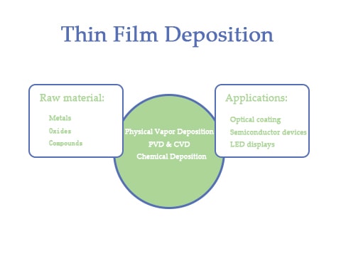
Thin film deposition is a process that is used to create thin films of different materials. Thin films can be put on different surfaces. Thin films can have metals, semiconductors, and dielectrics in them. Thin films have different properties. Optical transmission, electrical insulation, and resistance to wear and corrosion are some of the properties of thin films.
One common use for thin film deposition is to create optical coatings. Optical coatings are used to improve the performance of optical devices by reducing losses from reflection and scattering. They can also protect optical components from being damaged by environmental factors like dust and moisture.
Thin film deposition is a process that is commonly used to make semiconductor devices. Thin films can be put onto different types of materials to create barriers or contacts between them. You can also control the thickness and composition of the films to get different electronic properties from the device.
Thin film deposition is also used to make LED displays. In this application, thin films of light-emitting or light-absorbing materials are put onto a surface. You can control the thickness and composition of these films to change the color of the display.
Which Materials Are Used in Thin Film Deposition?
Some of the most common materials used in thin film deposition are metals, oxides, and compounds. Each of these materials has its own unique benefits and drawbacks when it comes to thin film deposition.
- Metals
Metals are often used in thin film deposition because they are strong and durable. They can also be easily deposited onto a substrate material, making them a popular choice for many applications. However, metals can also be quite expensive, which can limit their use in some applications.
- Oxides
Oxides are another popular choice for thin film deposition. They are often used because they are very durable and can withstand high temperatures. They can also be deposited at relatively low temperatures, making them a good choice for many applications. However, oxides can also be brittle and difficult to work with, which can limit their use in some cases.
- Compounds
There are many reasons to use compounds in thin film deposition. They are strong and durable, and they can be deposited at relatively low temperatures. This makes them a good choice for many applications. However, compounds can also be expensive and difficult to work with, which can limit their use in some cases.
The choice of material for a thin film coating depends on the application it is being used for. Metals are good for thermal and electrical conduction, oxides are good for protection, and compounds can be tailored to have specific properties. Ultimately, the best material for a given application will depend on the specific needs of the project.
Main Types of Thin Film Deposition?
There are two main types of thin film deposition: chemical deposition and physical vapor deposition.
In chemical deposition(CVD), a thin film is deposited by reacting two or more substances. This process is used to deposit materials with low melting points, such as polymers and organics.
In physical vapor deposition(PVD), a thin film is deposited by heating a material to its boiling point and then condensing the vapor onto a surface. This process is used to deposit materials with high melting points, such as metals, ceramics, and semiconductors.
The two most common techniques of physical vapor deposition(PVD) are thermal evaporation and sputtering. Thermal evaporation is a process in which a material is heated until it vaporizes and the vapor is then deposited on a surface. Both thermal evaporation and sputtering can be used to deposit thin films of metal, metal alloys, and ceramics.
How Can You Get the Best Thin Film Deposition Possible?
In order to produce thin films with good properties, we need to use high-quality sputtering targets and evaporation materials. A number of factors can affect the quality of a sputtering target or evaporation material, including purity, grain size, and surface condition.
The purity of a sputtering target or evaporation material is important because impurities can cause defects in the thin film. The grain size is also important because larger grains can lead to poor film properties. The surface condition is important because rough surfaces can cause defects in the film.
In order to get the highest quality sputtering targets and evaporation materials, it is important to select materials that have high purity, small grain size, and smooth surfaces.
We have the resources and team to help you with your production process. If you need evaporation materials or sputtering targets, we can help you choose the best option for your project. Contact us today!