


 +86-731-89578196
 [email protected]


- Home
- Our Company
-
Products
Sputtering Targets
- Industries
- Blog
- FAQ
- Contact Us

Magnetron Sputtering: The Smart Solution for Thin Film Innovation
Magnetron sputtering is a vital thin film deposition technique used across electronics, optics, energy, and many high-tech industries. It's fast, efficient, and highly controllable, making it a go-to method for researchers and manufacturers.
At AEM Deposition, we've built our reputation around providing the high-purity sputtering targets that make this process possible. By combining deep material knowledge with global service, we help our customers achieve precise outcomes in every layer they build.
Let's explore why magnetron sputtering continues to be the preferred technique for modern thin film deposition—and how AEM is supporting engineers, scientists, and manufacturers around the world.
Magnetron Sputtering: A Powerful Thin Film Deposition Method
So, how does this process really compare to other deposition methods?
Unlike traditional coating approaches that rely on chemical reactions, high heat, or evaporative techniques, magnetron sputtering works in a vacuum using plasma and magnetic fields. This makes it not only cleaner and more controlled but also suitable for a wider range of materials and surfaces.
For example, evaporation deposition may struggle with complex material compositions or produce non-uniform layers on large substrates. In contrast, sputtering offers better step coverage, excellent adhesion, and the ability to deposit alloys or compound films with precise control over stoichiometry.
More importantly, magnetron sputtering can be scaled. It's just as effective in a university lab working on a proof-of-concept as it is on an industrial production line depositing coatings over large areas with high throughput.
In short, magnetron sputtering isn't just a tool. It's a bridge between material performance and application success.
Why Magnetron Sputtering Is Essential in Modern Manufacturing
What makes magnetron sputtering stand out? Here's why manufacturers, labs, and research facilities swear by it:
- Uniform Coating: Delivers precise, consistent thin films.
- Material Versatility: Works with metals, ceramics, and composites.
- Scalability: Ideal for both research-scale and large-scale production.
- Cost-Effective: Low material waste compared to other techniques.
It’s no wonder that companies and institutions globally have adopted it as a core part of their fabrication processes.
How Magnetron Sputtering Actually Works
While the word “sputtering” might sound a bit chaotic, the process is anything but. At its core, magnetron sputtering is a highly engineered technique for converting solid material into vapor and guiding it to a new surface with microscopic precision.
Here’s how it unfolds:
-
Step 1: Vacuum and Gas Introduction
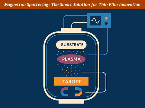
The process starts inside a sealed vacuum chamber, where air is removed to prevent contamination. Then, an inert gas—typically argon—is introduced.
-
Step 2: Plasma Generation
A power supply sends a high voltage through the chamber, ionizing the gas and creating a glowing plasma. This plasma is full of positively charged ions and free electrons.
-
Step 3: Ion Bombardment
These ions are drawn toward the negatively charged sputtering target, which contains the material to be deposited. Upon impact, they dislodge atoms from the surface of the target—this is the sputtering effect.
-
Step 4: Film Formation
The freed atoms travel across the vacuum chamber and condense onto the substrate (the material being coated), forming a thin and uniform layer.
-
Step 5: Magnetic Enhancement
Here’s where the “magnetron” comes in. Magnets placed behind the target trap electrons near the surface, increasing the ionization rate of the gas and thus boosting the efficiency of the process. This results in higher deposition rates, lower substrate heating, and better control.
One of the beauties of magnetron sputtering is its flexibility. You can tailor the process for different materials, film thicknesses, surface finishes, and substrate shapes. By adjusting parameters like power input, gas pressure, and magnetic field strength, technicians can fine-tune deposition rates and film characteristics in real time.
This isn’t just useful—it’s critical. For industries like microelectronics, where a few atoms' difference can impact conductivity or capacitance, magnetron sputtering delivers the kind of repeatable, scalable precision that no other method quite matches.
Key Components of a Magnetron Sputtering System
To get optimal performance, every part of the system matters. The major components include:
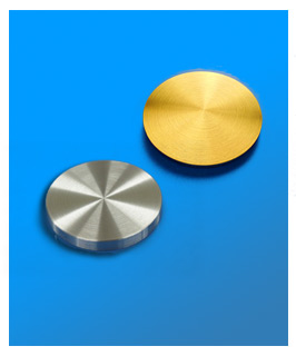
- Sputtering Target: The source of the thin film material.
- Substrate: The surface being coated.
- Magnetron Cathode: Holds the target and magnets.
- Power Supply: Delivers energy to create plasma (DC or RF).
- Vacuum Chamber: Keeps the environment contamination-free.
Each element must work in harmony to ensure high-purity, uniform coatings.
DC vs. RF Magnetron Sputtering: What's the Difference?
Choosing between DC (Direct Current) and RF (Radio Frequency) magnetron sputtering isn’t just a technical decision—it’s a strategic one that affects coating performance, production efficiency, and even cost.
Let’s break it down.
DC Magnetron Sputtering
This method is best suited for conductive targets, such as metals. It uses a constant negative voltage applied to the target, which accelerates positive gas ions toward it. These ions knock atoms off the target, and those atoms then coat the substrate.
Because of its simplicity, DC sputtering tends to be:
- Faster in deposition rate
- More energy-efficient
- Easier to scale for high-volume manufacturing
For example, if you’re depositing aluminum, titanium, or copper, DC sputtering is often the go-to choice. It’s ideal for applications where electrical conductivity and high deposition speed are priorities.
RF Magnetron Sputtering
Things get more complex with non-conductive materials—such as ceramics, oxides, or nitrides. These can build up electrical charge on the surface during DC sputtering, leading to arc discharges and process instability.
RF sputtering solves this by alternating the polarity at high frequencies (usually 13.56 MHz). This alternation allows charge to neutralize, enabling smooth and stable sputtering of insulators.
Use RF sputtering for:
- Transparent conductive oxides (like ITO or ZnO)
- Hard coatings (like TiN or AlN)
- Dielectric layers in semiconductors
At AEM Deposition, we help customers choose the right method based on their material, system setup, and film requirements. If needed, we even guide them on hybrid systems—some chambers use dual power sources to deposit multi-layer stacks in a single run.
In essence, your power strategy should be just as carefully selected as your target material.
Common Materials Used in Magnetron Sputtering
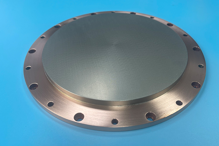
Each sputtering project begins with a question:
-
ITO (Indium Tin Oxide) for touchscreen transparency -
Al₂O₃ for dielectric coatings -
ZnO for piezoelectric applications
Nitrides and Carbides:
Known for their toughness, nitrides and carbides offer wear resistance and thermal stability. Think:
- TiN (Titanium Nitride) for cutting tools
- SiC (Silicon Carbide) for power electronics
- CrN for decorative, anti-corrosion coatings
Alloys and Composites
Sometimes, single-element targets can't achieve the performance needed. That's where engineered targets come in—custom alloys, mixed oxides, doped ceramics—made to order.
AEM Deposition: Your Trusted Sputtering Target Supplier
At AEM Deposition, we are more than just a manufacturer. We're your partner in precision thin film technology. Here's what sets us apart:
- Decades of Experience in materials science
- In-house production with ISO-certified processes
- Global logistics: Fast shipping, secure packaging
- Expert support: We help you succeed from spec to sputter
Our clients include universities, Fortune 500 companies, and government labs.
At AEM Deposition, we manufacture and supply:
- Pure targets from 99.9% up to 99.9999%
- Alloys designed for specific optical, thermal, or mechanical outcomes
- Bonded targets for high-power sputtering
- Unusual shapes and complex geometries
Every target is crafted with precision: homogeneous structure, clean surfaces, and tight tolerances. The choice of material directly affects film properties like conductivity, hardness, and transparency.
Conclusion: Thin Film Excellence Starts with the Right Target
As technology keeps advancing, magnetron sputtering will only grow in importance. Whether you're developing new materials or scaling production, the right sputtering target is key.
Magnetron sputtering is the backbone of countless technologies. And like any high-precision process, its success hinges on the materials you feed it.
With AEM Deposition, you get more than just sputtering targets—you get a team of experts, decades of experience, and a commitment to excellence.
Let's make your next breakthrough possible.
Contact us today to request a quote or consultation.