 +86-731-89578196
 [email protected]
- Home
- Our Company
-
Products
Sputtering Targets
- Industries
- Blog
- FAQ
- Contact Us
Understanding the Difference: N-Type vs P-Type Semiconductors
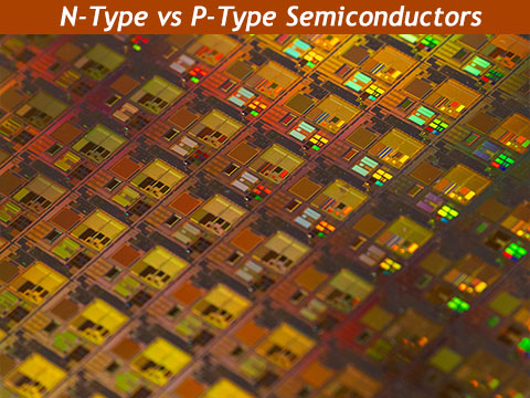
Welcome to the world of semiconductors, where tiny components hold the power to revolutionize our lives. Among these components, N-type and P-type semiconductors play a crucial role in shaping the future of technology.
But what exactly sets them apart? In this article, we will delve into the intricacies of these two semiconductor types and understand their differences. N-type semiconductors are known for their abundance of free electrons, making them highly conductive. On the other hand, P-type semiconductors possess an excess of positively charged holes, resulting in a lower conductivity compared to N-type.
Exploring their unique characteristics and contrasting properties will shed light on their applications in various electronic devices. Whether you are a tech enthusiast or a curious learner, join us as we unravel the fascinating world of N-type and P-type semiconductors and discover the impact they have on our digital landscape.
Basic principles of semiconductor materials
Semiconductors are materials that have electrical conductivity between conductors (such as metals) and insulators (such as non-metals). They are essential for the functioning of electronic devices. The behavior of semiconductors is based on the movement of electrons within their atomic structure.
In a pure semiconductor, the atoms are arranged in a crystal lattice, and each atom contributes a certain number of electrons to the material's conduction band. However, impurities or dopants can be intentionally added to alter the conductivity properties of the semiconductor. This is where N-type and P-type semiconductors come into play.
What are N-type semiconductors?
N-type semiconductors are formed by adding impurities that introduce excess electrons into the crystal lattice. These impurities are known as donor impurities. The most commonly used donor impurity is phosphorus, which has an extra electron compared to the host semiconductor material, such as silicon.
This additional electron becomes a free electron in the crystal lattice, contributing to the conductivity of the material. N-type semiconductors are characterized by an abundance of free electrons, which allow for efficient electron flow. The presence of these free electrons makes N-type semiconductors highly conductive.
Properties and characteristics of N-type semiconductors
N-type semiconductors have several unique properties and characteristics that make them suitable for specific applications. Firstly, their high conductivity makes them ideal for use in electronic components that require efficient electron flow, such as transistors and diodes.
N-type semiconductors also exhibit a negative charge, as the excess of electrons creates an overall negative charge in the material. This negative charge is crucial for certain electronic devices, as it enables the manipulation of electric current.
Additionally, N-type semiconductors have a relatively low resistance, allowing for the easy flow of electric current.
What are P-type semiconductors?
P-type semiconductors are formed by adding impurities that create an excess of positively charged holes in the crystal lattice. These impurities are known as acceptor impurities.
The most commonly used acceptor impurity is boron, which has one less electron compared to the host semiconductor material. This missing electron creates a hole in the crystal lattice, which acts as a positive charge carrier.
P-type semiconductors are characterized by the presence of these holes, which contribute to the conductivity of the material. However, due to the absence of free electrons, P-type semiconductors have lower conductivity compared to N-type.
Properties and characteristics of P-type semiconductors
P-type semiconductors possess unique properties and characteristics that make them valuable in various electronic applications.
Firstly, their lower conductivity makes them suitable for devices that require a controlled flow of electric current. P-type semiconductors exhibit a positive charge, as the presence of holes creates an overall positive charge in the material.
This positive charge is crucial for specific electronic devices, as it allows for the manipulation of electric current. Additionally, P-type semiconductors have a relatively high resistance, which can be advantageous in specific applications that require precise control over the flow of electric current.
The key difference between N-type and P-type semiconductors
The key difference between N-type and P-type semiconductors lies in their conductivity, charge carriers, and energy band diagrams.
Conductivity differences
The conductivity of a semiconductor is determined by the density and mobility of its charge carriers. In N-type semiconductors, the extra electrons introduced by the doping process are the dominant charge carriers. These electrons are relatively free to move within the crystal lattice, contributing to the high conductivity of N-type materials.
In P-type semiconductors, the dominant charge carriers are the holes created by the doping process. While holes are often referred to as positive charge carriers, it is important to note that they are actually the absence of an electron in the valence band. Despite this, holes behave as if they were positively charged particles, allowing them to move through the crystal lattice and contribute to the conductivity of P-type materials.
The differences in conductivity between N-type and P-type semiconductors are crucial in the design and operation of electronic devices. By strategically combining N-type and P-type materials, it is possible to create diodes, transistors, and other electronic components that utilize these conductivity differences to control the flow of current.
Charge carriers
N-type semiconductors have an abundance of free electrons, which contribute to their high conductivity.
On the other hand, P-type semiconductors possess an excess of positively charged holes, resulting in a lower conductivity compared to N-type. This difference in charge carriers leads to contrasting behavior in electronic devices. N-type semiconductors allow for the easy flow of electrons, while P-type semiconductors facilitate the movement of holes. These unique characteristics make N-type and P-type semiconductors suitable for different applications in electronic devices.
Energy band diagrams
To better understand the behavior of N-type and P-type semiconductors, it is helpful to visualize their energy band diagrams. In an energy band diagram, the energy levels of electrons in the material are represented by bands, with the valence band being the band closest to the nucleus and the conduction band being the band further away.
In N-type semiconductors, the extra electrons introduced by the doping process occupy the conduction band, which is separated from the valence band by an energy gap. This energy gap is relatively small, allowing the electrons to move easily from the valence band to the conduction band, contributing to the high conductivity of N-type materials.
In P-type semiconductors, the energy band diagram is slightly different. The holes created by the doping process occupy the valence band, while the conduction band remains empty. This creates a relatively large energy gap between the valence and conduction bands, making it more difficult for electrons to move from the valence band to the conduction band. However, when a voltage is applied across a P-type semiconductor, the electrons from the N-type material can fill the holes in the valence band, allowing current to flow.
Applications of N-type and P-type semiconductors
The distinct properties of N-type and P-type semiconductors make them invaluable in various electronic devices. N-type semiconductors are commonly used in transistors, diodes, and integrated circuits, where efficient electron flow is crucial.
They are also utilized in photovoltaic cells, as the abundance of free electrons enables efficient conversion of light energy into electrical energy.
P-type semiconductors, on the other hand, find applications in devices such as solar cells, where the movement of holes is essential for generating an electric current. They are also utilized in diodes and bipolar junction transistors, which require a controlled flow of electric current.
Importance of understanding N-type and P-type semiconductors in technology
Understanding the differences between N-type and P-type semiconductors is vital for anyone involved in the field of technology. Electronic devices and circuits rely on the precise manipulation of electric current, and the choice of semiconductor material plays a crucial role in achieving this control.
By comprehending the characteristics and behavior of N-type and P-type semiconductors, engineers and scientists can design and optimize electronic components for specific applications. This knowledge is essential for advancements in fields such as telecommunications, renewable energy, and computing. Furthermore, understanding the intricacies of N-type and P-type semiconductors allows for the development of more efficient and innovative electronic devices.
Conclusion
N-type and P-type semiconductors are the fundamental building blocks of modern electronics. Their unique characteristics and behavior have allowed for the development of a wide range of electronic devices that have transformed the way we live and work. From transistors and diodes to solar cells and thermoelectric devices, N-type and P-type semiconductors continue to drive technological advancements.
While challenges and limitations exist, ongoing research and development in the field of semiconductor technology hold the promise of overcoming these hurdles and unlocking even greater potential. As we continue to push the boundaries of what is possible, the world of N-type and P-type semiconductors will undoubtedly play a central role in shaping the future of technology.
At our company, we offer a range of products to support the development and manufacturing of semiconductors. Our sputtering targets and semiconductor substrates and wafers are designed to meet the needs of researchers and manufacturers alike. For more information on our products, please contact us.


