


 +86-731-89578196
 [email protected]

- Home
- Our Company
-
Products
Sputtering Targets

- Industries
- Blog
- FAQ
- Contact Us


Application of Chemical Vapor Deposition in Semiconductor Films
views, Updated: 2021-09-20
Chemical vapor deposition (CVD) is a well-known technology in the field of nanomanufacturing. Through the use of gas-to-gas reactions, CVD can deposit evaporated reactants on the surface to form thin-films. Therefore, CVD can be applied to semiconductor films.
Application of vapor deposition in semiconductor films
At present, CVD can be used in many monoatomic materials, such as graphene, which is composed of carbon atoms. But for semiconductor materials, the process can be more complex because they usually contain multiple metal atoms. For example, "Silicon", which is one of the earliest (and simplest) semiconductor materials are known, can be produced by silane (SiH4) in a chemical vapor deposition reactor system.
If we want to make more complex semiconductor films, such as GaAs or GaN films, we need to use MOCVD. Like many other CVD technologies, MOCVD is an extension and improved version of CVD technology. In this process, ultra-pure gas is injected into the reactor, and the very thin atomic layer is deposited on the semiconductor wafer after fine measurement. The surface reaction of organic compounds or metal organics containing the required chemical elements and hydrides creates conditions for crystal growth, forming the epitaxy of materials and compound semiconductors. Unlike traditional silicon semiconductors, these semiconductors can contain elements in combination with groups III and V, II and VI, IV or IV, V and VI.
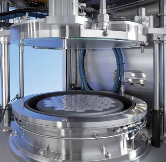
MOCVD reaction chamber
In addition, the deposition temperature of MOCVD is relatively low, so it has a high application value for those substrates which can not bear the high-temperature of conventional CVD but need to use medium and low-temperature matrix (such as steel matrix). In addition to Gan and other materials, the polycrystalline SiO2 grown by MOCVD technology is a good transparent conductive material. The TiO2 crystalline film obtained by MOCVD is used in the anti-reflection layer, water photolysis, and photocatalysis of solar cells.
LATEST NEWS