


 +86-731-89578196
 [email protected]

- Home
- Our Company
-
Products
Sputtering Targets

- Industries
- Blog
- FAQ
- Contact Us


Surface Treatment Process of Physical Vapor Deposition (Attached Figure)
views, Updated: 2021-09-20
Physical vapor deposition refers to the deposition of the evaporated material and its reaction products on the workpiece by using the arc discharge technology of low voltage and high current under the vacuum condition, using the gas discharge to evaporate the target and ionize the evaporated material and gas, and using the acceleration of electric field.
The main methods of PVD are vacuum evaporation, sputtering, arc plasma, ion, and MBE. At present, physical vapor deposition technology can deposit metal films, alloy films, compounds, ceramics, semiconductors, polymer films.
So, what is the process of physical vapor deposition? Take a look at the following figure:
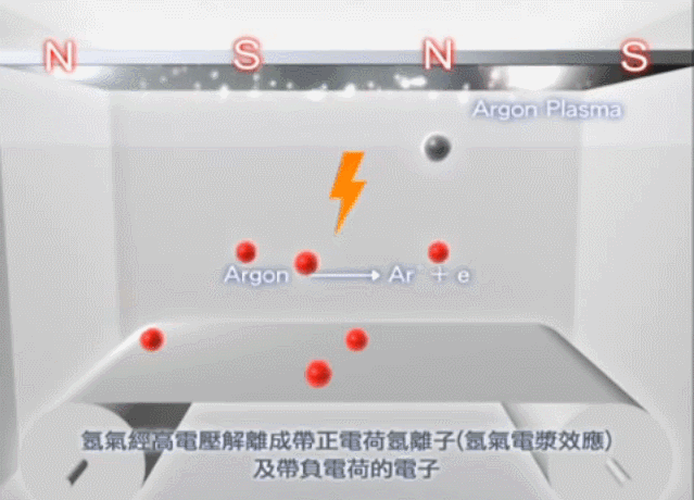
From the above diagrams, we can see that argon dissociates into positively charged argon ions (argon plasma effect) and negatively charged electrons through high voltage. It is finally deposited on the surface of the workpiece.
If this is difficult to understand, please send us an email for further communication. We (AEM Deposition) is an international company involved in the R & D, manufacturing, and sales of all kinds of high-tech materials. We provide high-purity non-ferrous materials, customized alloys, compounds, and almost every kind of complicated synthetic materials to research institutes and high-tech enterprises worldwide. We have significant advantages in magnetron sputtering targets, vacuum coating materials, high-purity metals, high-purity compounds, rare-earth metals, distilled rare-earth metals, coated substrates, along with many other materials.
LATEST NEWS