


 +86-731-89578196
 [email protected]


- Home
- Our Company
-
Products
Sputtering Targets
- Industries
- Blog
- FAQ
- Contact Us
ALD Coating Explained: Process, Applications, and Materials for Advanced Thin Films
views, Updated: 2026-07-09
Introduction: The Role of ALD Coating in Advanced Thin Film Manufacturing
Modern electronic devices are becoming smaller and more powerful. As semiconductor technology continues to advance, manufacturers need thin films with better thickness control, higher uniformity, and improved reliability.
However, applying high-quality coatings on extremely small and complex structures is becoming more challenging. Traditional deposition methods may have limitations when coating deep structures, narrow spaces, or nanoscale features.
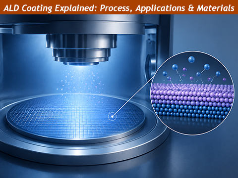
ALD coating (Atomic Layer Deposition coating) provides an effective solution for these challenges. It is an advanced thin film deposition technology that builds coatings in very thin layers through controlled chemical reactions. This allows manufacturers to create uniform films with precise thickness control.
Due to its excellent coating performance, ALD is widely used in semiconductor manufacturing, including advanced memory devices and logic components. It is also applied in areas such as MEMS, optical devices, batteries, and protective coatings.
In this article, we will explain what ALD coating is, how the ALD process works, its key advantages, major applications, and the materials commonly used in advanced thin film manufacturing.
What Is ALD Coating?
ALD coating (Atomic Layer Deposition coating) is an advanced thin film deposition technology that creates coatings by controlling chemical reactions on a surface.
Unlike some traditional deposition methods that continuously deposit materials onto a substrate, ALD builds a film through repeated cycles. During each cycle, a very thin layer of material is formed on the surface. By controlling the number of cycles, manufacturers can adjust the final coating thickness with high accuracy.
The main feature of ALD is its ability to produce highly uniform films, even on complex surfaces. Because the coating process is carefully controlled, ALD can cover areas that are difficult to reach with conventional methods, such as tiny structures and high aspect ratio features.
Compared with other thin film technologies, ALD is especially suitable for applications that require:
· Precise thickness control
· Excellent surface coverage
· High-quality and reliable thin films
These advantages make ALD an important technology in advanced semiconductor manufacturing and other high-performance applications.
How Does ALD Coating Work?
Unlike many traditional deposition methods, ALD coating does not build a film by depositing a large amount of material at once. Instead, it grows the coating through repeated surface reactions, adding a very thin layer during each cycle.
The ALD process is based on two different chemical precursors that react with the surface separately. Because each reaction is carefully controlled, the film grows in a predictable and uniform way.
A typical ALD cycle includes four main steps:
Step 1: Introducing the First Precursor
The first precursor is introduced into the reaction chamber and reaches the substrate surface.The precursor reacts with the available sites on the surface. Once the surface is fully covered, the reaction naturally stops. This prevents excessive material growth and allows precise control of each layer.
Step 2: Removing Excess Materials
After the first reaction is complete, an inert gas is used to clean the reaction chamber.This removes unused precursor molecules and reaction by-products, ensuring that the next step starts with a clean surface.
Step 3: Adding the Second Precursor
The second precursor is then introduced into the chamber.It reacts with the first layer formed on the surface and creates the desired thin film material. Similar to the first step, the reaction stops after the surface reaches a stable condition.
Step 4: Completing One ALD Cycle
A second cleaning step removes remaining gases and by-products from the chamber.After one complete cycle, only a very thin film layer has been deposited. By repeating the cycle many times, manufacturers can build coatings with the required thickness while maintaining excellent uniformity.
Example: ZrO₂ Thin Film Deposition
Zirconium oxide (ZrO₂) is one example of a material that can be produced using ALD technology.During the process:
· A zirconium-based precursor is introduced first.
· An oxidizing agent reacts with the surface layer.
· A thin ZrO₂ film is formed after each cycle.
· Repeating the cycles increases the final film thickness.
This controlled growth process allows ALD to produce high-quality coatings with accurate thickness and excellent coverage, which is why it is widely used in advanced semiconductor and thin film applications.
Why Is ALD Coating Important for Advanced Thin Films?
As electronic devices become smaller and more advanced, manufacturers need better ways to create thin and reliable coatings. ALD coating provides several advantages that make it suitable for modern thin film applications.
Precise Thickness Control
ALD can create very thin films with accurate thickness control. By adjusting the number of ALD cycles, manufacturers can achieve the required coating thickness for different applications.This is especially important in semiconductor manufacturing, where even small changes in film thickness can affect device performance.
Excellent Coverage on Complex Structures
Many advanced devices contain tiny features and three-dimensional structures that are difficult to coat evenly.ALD can provide uniform coatings on complex surfaces, including narrow spaces and high aspect ratio structures. This makes it useful for applications such as advanced memory chips and semiconductor devices.
High-Quality and Reliable Thin Films
ALD helps produce thin films with good uniformity and stable performance.These high-quality coatings can improve the reliability of electronic components and support the development of advanced technologies.
Suitable for Future Manufacturing Needs
As industries continue to demand smaller and more powerful devices, thin film requirements are becoming more challenging.With its precise coating control and excellent surface coverage, ALD will continue to play an important role in semiconductor, optical, energy, and other advanced applications.
ALD Coating Applications in Advanced Industries
ALD coating is widely used in industries that require precise, uniform, and high-quality thin films. Among these applications, semiconductor manufacturing is the most important area, while ALD is also used in optical devices, sensors, and protective coatings.
Semiconductor Manufacturing
Semiconductor manufacturing is the largest application area for ALD coating. As chip structures become smaller and more complex, ALD helps manufacturers create thin films with accurate thickness control and excellent surface coverage.Common ALD materials include:
· Hafnium oxide (HfO₂)
· Zirconium oxide (ZrO₂)
· Aluminum oxide (Al₂O₃)
· Titanium nitride (TiN)
These materials are used for applications such as:
· High-k dielectric layers
· Gate structures
· Barrier layers
· Advanced memory devices including DRAM and 3D NAND
The ability to coat complex nanoscale structures uniformly makes ALD an important technology for next-generation semiconductor devices.
Optical and Display Applications
ALD is also used in optical and display technologies to create functional thin films.For example, transparent conductive oxide (TCO) coatings such as ZnO and In₂O₃ can be applied in applications including OLED displays and solar cells.
These coatings help improve electrical performance, optical properties, and device stability.
MEMS and Sensor Applications
In MEMS and sensor manufacturing, ALD can provide uniform coatings on small and complex structures.It is used in applications such as:
· Gas sensors
· Pressure sensors
· Biosensors
ALD coatings can improve surface performance, sensitivity, and device reliability.
Protective Coatings
ALD can also enhance the surface properties of different materials by creating thin protective layers.These coatings can improve:
· Wear resistance
· Corrosion resistance
· Surface durability
They are used for mechanical components, biomedical devices, and other applications that require long-term material protection.
Summary
With its precise thickness control and excellent coating uniformity, ALD has become an important technology for semiconductor manufacturing and other advanced applications. As industries continue to demand higher-performance materials and thinner films, ALD will continue to play a key role in future thin-film technologies.Common Materials Used for ALD Thin Films
ALD coating can be used to deposit a wide range of thin film materials with different electrical, optical, and mechanical properties. The selection of material depends on the requirements of the final application, such as insulation, conductivity, protection, or surface modification.It is important to note that ALD uses chemical precursors rather than solid sputtering targets as the material source. The materials below refer to the thin films formed by the ALD process, which are widely used in advanced semiconductor and coating applications.
Aluminum Oxide (Al₂O₃)
Aluminum oxide is one of the most commonly used ALD materials due to its excellent dielectric properties and chemical stability.Typical applications include:
· Insulating layers in semiconductor devices
· Surface protection coatings
· Barrier films for preventing moisture and chemical penetration
Its good uniformity and reliability make Al₂O₃ suitable for many thin film applications.
Hafnium Oxide (HfO₂)
Hafnium oxide is an important high-k dielectric material used in advanced semiconductor manufacturing.Key advantages include:
· High dielectric constant
· Good thermal stability
· Excellent electrical performance
HfO₂ ALD films are commonly used in:
· Gate dielectric layers
· Advanced logic devices
· Semiconductor memory applications
Zirconium Oxide (ZrO₂)
Zirconium oxide is another important oxide material used in ALD processes.It offers:
· High chemical stability
· Good dielectric properties
· Strong temperature resistance
ZrO₂ thin films are used in applications such as:
· Memory devices
· Functional oxide layers
· Advanced electronic components
Titanium Nitride (TiN) and Other Metal Nitride Films
Metal nitride films are widely used in advanced thin film applications because they provide excellent electrical, thermal, and chemical stability.Titanium nitride (TiN) is one of the most important ALD materials in semiconductor manufacturing. It combines good electrical conductivity with strong resistance to heat and chemical environments, making it suitable for:
· Barrier layers
· Gate electrodes
· Semiconductor interconnect structures
Other metal nitride materials, such as aluminum nitride (AlN), are also used in applications that require high thermal stability and protective performance.
The excellent durability and functional properties of metal nitride films make them valuable materials for advanced electronic devices and high-performance coating applications.
Summary
From dielectric films to conductive layers, ALD materials play an important role in producing high-performance thin films. Choosing the right material is essential for achieving the required electrical, mechanical, and chemical properties in advanced applications.ALD Coating vs Other Thin Film Deposition Technologies
ALD, PVD, and CVD are all important thin film deposition technologies, but they are designed for different application requirements. The right choice depends on factors such as film thickness, structure complexity, coating uniformity, and production efficiency.
| Feature | ALD Coating | PVD / Sputtering | CVD |
|---|---|---|---|
| Deposition mechanism | Surface chemical reactions | Physical atom transfer from a solid target | Gas-phase chemical reactions |
| Film growth | Layer-by-layer growth | Direct material deposition | Continuous film growth |
| Thickness control | Excellent, controlled by deposition cycles | Good, controlled by deposition time | Good, controlled by process conditions |
| Surface coverage | Excellent, especially for complex 3D structures | Limited to high aspect ratio structures | Good |
| Deposition speed | Slow | Fast | Faster than ALD |
| Typical temperature | Usually lower | Low to moderate | Usually higher |
| Main advantages | Atomic-level control and excellent conformality | High deposition rate and wide material selection | Good film quality and industrial scalability |
| Common applications | Advanced semiconductors, nanoscale coatings | Displays, semiconductor films, optical coatings | Semiconductor layers, industrial coatings |
ALD vs Sputtering
ALD and sputtering are complementary thin-film technologies.ALD is preferred when applications require:
· Extremely thin films
· Precise thickness control
· Uniform coating on complex structures
Sputtering is preferred when manufacturers need:
· Higher deposition speed
· Large-area coating
· A wide range of metal, alloy, and ceramic films
For example, ALD may be used to create ultra-thin functional layers in advanced semiconductor devices, while sputtering is commonly used for metal films, electrodes, and optical coatings.
ALD vs CVD
Both ALD and CVD use chemical reactions to form thin films, but the processes are different.CVD introduces reactive gases into the chamber at the same time, allowing continuous film growth. ALD separates the reactions into individual cycles, providing better thickness control and surface coverage.
Therefore:
· CVD is often suitable for faster deposition and larger-scale production.
· ALD is better for nanoscale applications requiring precise and uniform coatings.
Choosing the Right Deposition Method
There is no single "best" deposition technology for all applications. Manufacturers select the appropriate method based on:· Required film thickness
· Substrate structure
· Material requirements
· Production efficiency
· Cost considerations
In advanced manufacturing, different deposition technologies often work together to achieve the desired film performance.
Conclusion
ALD coating has become an important technology for making advanced thin films. Its ability to create precise and uniform coatings helps manufacturers build smaller and more powerful devices.
As industries continue to develop new technologies, the demand for better thin film solutions will continue to grow. ALD provides a reliable option for applications that require accurate thickness control and high-quality coatings.
Choosing the right deposition technology and materials is also important for achieving stable results. AEM Deposition® provides customized sputtering targets, evaporation materials, and high-purity materials for semiconductor, optical, and research applications.
LATEST NEWS