


 +86-731-89578196
 [email protected]

- Home
- Our Company
-
Products
Sputtering Targets

- Industries
- Blog
- FAQ
- Contact Us


Ion Beam Sputtering Process and Target Material Requirements
views, Updated: 2026-06-23
Introduction
Ion Beam Sputtering (IBS) is one of the most precise thin-film deposition technologies used today. It is widely applied in optical coatings, semiconductor devices, aerospace optics, and advanced research applications where film quality and process control are critical.Compared with many conventional deposition methods, IBS offers excellent control over film thickness, density, composition, and surface roughness. These advantages make it a preferred choice for applications that require highly uniform and low-defect coatings.
However, achieving consistent coating performance depends on more than the deposition equipment itself. The quality of the sputtering target, including its purity, density, and microstructure, can have a significant impact on deposition stability and film properties.
In this article, we explain how ion beam sputtering works, compare it with magnetron sputtering, and discuss the key target material requirements for high-performance IBS applications.
What Is Ion Beam Sputtering?
Ion Beam Sputtering (IBS) is a physical vapor deposition (PVD) process used to produce high-quality thin films. Unlike conventional sputtering methods that rely on plasma generated near the target, IBS uses a dedicated ion source to create and accelerate ions toward the target material.When high-energy ions, typically argon ions, strike the target surface, atoms are ejected from the target. These atoms then travel through the vacuum chamber and deposit onto the substrate, forming a thin and uniform coating.
One of the main advantages of ion beam sputtering is the ability to independently control the ion beam. Parameters such as ion energy, beam current, and incident angle can be adjusted with high precision, allowing better control over the deposition process and film properties.
As a result, IBS can produce coatings with:
· High film density
· Excellent thickness uniformity
· Low surface roughness
· Minimal contamination
· Precise composition control
Because of these characteristics, ion beam sputtering is widely used in applications where coating quality is more important than deposition speed, including optical coatings, semiconductor devices, aerospace optics, and advanced research materials.
Ion Beam Sputtering vs Magnetron Sputtering
Both ion beam sputtering and magnetron sputtering are widely used thin film deposition technologies, but they are designed for different priorities.Ion beam sputtering focuses on precision and film quality. The ion beam is generated separately from the target, providing greater control over the sputtering process and reducing interference from the plasma environment.
Magnetron sputtering, on the other hand, uses magnetic fields to increase plasma density around the target. This significantly improves deposition rates and makes it well suited for large-scale industrial production.
| Feature | Ion Beam Sputtering | Magnetron Sputtering |
|---|---|---|
| Deposition Precision | Excellent | Good |
| Film Density | Excellent | Good |
| Thickness Control | Excellent | Good |
| Deposition Rate | Lower | Higher |
| Target Utilization | Lower | Higher |
| Typical Applications | Precision optics, research, semiconductor devices | Large-area coatings, display panels, industrial production |
For applications that require extremely dense films, smooth surfaces, and precise thickness control, ion beam sputtering is often the preferred choice despite its lower deposition rate.
How the Ion Beam Sputtering Process Works
Ion beam sputtering uses a controlled beam of ions to remove atoms from a target material and deposit them onto a substrate. Although the equipment can be sophisticated, the basic process can be divided into four steps.Step 1: Ion Beam Generation
The process begins with an ion source that generates positively charged ions, typically argon ions (Ar⁺). These ions are accelerated by an electric field, creating a focused ion beam with a controlled energy level.Unlike magnetron sputtering, where ions are generated within a plasma near the target, IBS produces the ion beam separately. This allows more precise control of the deposition process.
Step 2: Target Bombardment
The accelerated ion beam is directed toward the sputtering target. When the ions strike the target surface, they transfer energy to the target atoms.If the transferred energy is high enough, atoms are ejected from the target material. This phenomenon is known as sputtering.
The sputtering rate depends on several factors, including:
· Ion energy
· Beam current density
· Target material properties
· Incident angle of the ion beam
Step 3: Material Ejection and Transport
After leaving the target surface, the sputtered atoms travel through the vacuum chamber toward the substrate.Because IBS operates under high-vacuum conditions, there are fewer collisions between atoms and gas molecules. This helps maintain a stable deposition process and allows the coating material to reach the substrate with minimal contamination.
Step 4: Thin Film Growth
The sputtered atoms condense on the substrate surface and gradually form a thin film.By controlling deposition parameters, engineers can precisely adjust film thickness, composition, density, and microstructure. This level of control is one reason why ion beam sputtering is widely used for high-performance optical and electronic coatings.
Why Process Control Matters
One of the biggest advantages of ion beam sputtering is its high level of process control. Several key parameters can be adjusted independently to optimize film performance:· Ion Energy: Influences sputtering efficiency and film density.
· Beam Current Density: Affects deposition rate and coating uniformity.
· Incident Angle: Impacts sputtering yield and film growth behavior.
· Deposition Time: Determines final film thickness.
Careful control of these parameters helps produce coatings with excellent uniformity, low defect levels, and highly consistent properties from batch to batch.
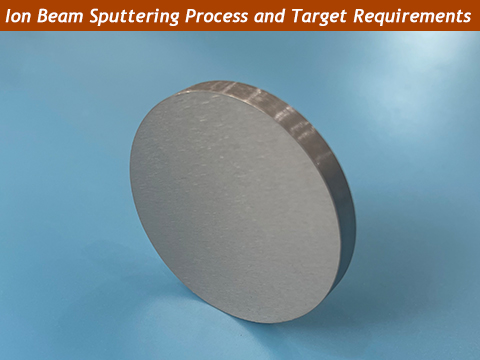
Key Target Material Requirements for Ion Beam Sputtering
Because ion beam sputtering relies on a focused beam of high-energy ions to remove material from the target surface, target quality has a direct impact on deposition performance and film properties. To achieve consistent results, IBS targets should meet several important requirements.High Purity
Purity is one of the most critical factors in sputtering target selection.Impurities in the target can be transferred to the deposited film, affecting its optical, electrical, or mechanical properties. In high-performance applications such as semiconductor devices and optical coatings, even trace contaminants can reduce product performance.
For this reason, sputtering targets are often manufactured with purities ranging from 99.95% to 99.999%, depending on the application requirements.
High Density
Target density affects sputtering stability and film quality.Low-density targets may contain pores or voids that can lead to uneven sputtering, particle generation, and inconsistent deposition rates. High-density targets help ensure a stable sputtering process and produce films with better uniformity and fewer defects.
This is particularly important in IBS, where coating quality is often a top priority.
Uniform Grain Structure
A uniform microstructure promotes consistent sputtering behavior across the entire target surface.Large variations in grain size can cause differences in sputtering rates, leading to non-uniform film thickness or composition. Carefully controlled manufacturing processes help produce targets with a homogeneous grain structure, improving deposition consistency.
Low Internal Defects
Internal cracks, inclusions, and voids can negatively affect both target performance and service life.Targets with minimal internal defects generally provide:
· More stable sputtering behavior
· Lower particle generation
· Better coating quality
· Longer operating life
Quality inspection methods such as ultrasonic testing and metallographic analysis are commonly used to verify internal integrity.
Precise Chemical Composition
Maintaining accurate chemical composition is especially important for alloy and ceramic targets.Even small variations in composition can affect film properties such as conductivity, refractive index, corrosion resistance, and mechanical performance. Consistent composition helps ensure reliable and repeatable coating results from batch to batch.
Strong Bonding to Backing Plates
Many sputtering targets are bonded to copper or aluminum backing plates to improve heat dissipation during operation.A strong and reliable bond helps:
· Improve thermal conductivity
· Reduce thermal stress
· Minimize the risk of target cracking
· Extend target service life
For large targets or high-power deposition systems, backing plate bonding can be an important factor in overall process stability.
By selecting targets with high purity, high density, uniform microstructure, and reliable bonding quality, manufacturers can achieve better deposition consistency, improved film performance, and higher production efficiency in ion beam sputtering applications.
Common Target Materials Used in Ion Beam Sputtering
Ion beam sputtering is compatible with a wide range of target materials, including metals, alloys, ceramics, and semiconductors. The choice of target depends on the required film properties, such as conductivity, optical performance, corrosion resistance, or thermal stability.Metal Targets
Metal targets are commonly used to deposit conductive, protective, and functional thin films.Popular metal targets include:
· Titanium (Ti) Target
· Tantalum (Ta) Target
· Niobium (Nb) Target
· Zirconium (Zr) Target
· Hafnium (Hf) Target
· Tungsten (W) Target
· Molybdenum (Mo) Target
· Nickel (Ni) Target
These materials offer excellent mechanical properties, corrosion resistance, and chemical stability. They are widely used in semiconductor manufacturing, optical coatings, and electronic devices.
For example, titanium and tantalum coatings are often used as adhesion layers and diffusion barriers in microelectronics, while hafnium-based coatings are valued for their high-temperature stability and dielectric properties.
Oxide Targets
Oxide targets are widely used to deposit optical, dielectric, and transparent conductive films.Common examples include:
· Indium Tin Oxide (ITO) Target
· Hafnium Oxide (HfO₂) Target
· Silicon Dioxide (SiO₂) Target
· Titanium Dioxide (TiO₂) Target
· Aluminum Oxide (Al₂O₃) Target
These materials are used in applications such as optical filters, display panels, solar cells, anti-reflection coatings, and protective dielectric layers.
In particular, ITO remains one of the most widely used transparent conductive materials for displays and touch-screen devices.
Semiconductor Targets
Semiconductor targets are used when precise electrical and optical properties are required.The most common materials include:
· Silicon (Si) Target
· Germanium (Ge) Target
Silicon targets are extensively used in semiconductor devices, optical coatings, and thin-film electronics. High-purity silicon targets are often required to ensure low defect levels and consistent film performance.
Material Selection Considerations
Selecting the right target material depends on the specific requirements of the coating application. Engineers typically consider factors such as:· Electrical conductivity
· Optical properties
· Thermal stability
· Corrosion resistance
· Film density requirements
· Deposition rate
· Cost and availability
In many high-performance IBS applications, material purity and target manufacturing quality are just as important as the material itself. A well-manufactured target helps ensure stable deposition behavior and consistent thin-film performance throughout the production process.
Typical Applications of Ion Beam Sputtering
Ion beam sputtering is typically used when coating quality, film density, and process control are more important than deposition speed. Its ability to produce highly uniform and low-defect films makes it valuable in several advanced industries.Precision Optical Coatings
One of the most important applications of ion beam sputtering is the production of high-performance optical coatings.IBS can create extremely dense and smooth films with precise thickness control, making it ideal for optical components that require high transmission, low scattering, and long-term stability.
Common applications include:
· Laser mirrors
· Optical filters
· Beam splitters
· Anti-reflection coatings
· Precision optical instruments
Because even small coating defects can affect optical performance, high-purity sputtering targets are often required for these applications.
Semiconductor and MEMS Devices
The semiconductor industry relies on thin films with precise composition and excellent uniformity.Ion beam sputtering is used to deposit metal, dielectric, and semiconductor films in applications where tight process control is essential. The technology is particularly useful for research, prototyping, and specialized semiconductor devices.
Typical applications include:
· Semiconductor thin films
· MEMS devices
· Sensors
· Microelectronic components
In these applications, target purity and composition consistency directly influence device performance and reliability.
Aerospace and Defense Optics
Many aerospace and defense systems operate in demanding environments where coating reliability is critical.Ion beam sputtering can produce coatings with excellent adhesion, durability, and environmental stability, making it suitable for advanced optical systems used in:
· Aerospace sensors
· Satellite optics
· Military imaging systems
· High-power laser equipment
The dense film structure produced by IBS helps improve long-term performance under harsh operating conditions.
Research and Advanced Materials Development
Universities, research institutes, and advanced manufacturing laboratories frequently use ion beam sputtering to develop and evaluate new thin-film materials.Because the process provides precise control over deposition parameters, researchers can accurately study the relationship between material composition, microstructure, and film properties.
Common research areas include:
· Thin-film electronics
· Optical materials
· Energy storage materials
· Functional coatings
· Emerging semiconductor technologies
For these projects, custom target compositions and specialized materials are often required to support experimental development.
Why IBS Is Chosen for These Applications
Although ion beam sputtering generally has a lower deposition rate than magnetron sputtering, it offers significant advantages when film quality is the primary concern.Manufacturers and researchers often choose IBS when they require:
· High film density
· Excellent thickness control
· Low surface roughness
· Precise composition control
· Superior optical or electronic performance
As a result, ion beam sputtering continues to play an important role in advanced coating applications where precision and reliability are essential.
Conclusion
Ion beam sputtering offers excellent control over thin-film deposition, making it ideal for high-performance optical, semiconductor, and research applications. To get the best results, it is important to use sputtering targets with high purity, high density, and consistent quality.Looking for a reliable sputtering target supplier? AEM offers custom metal, alloy, ceramic, and refractory metal targets designed to support stable deposition and high-quality thin-film production.
LATEST NEWS