


 +86-731-89578196
 [email protected]

- Home
- Our Company
-
Products
Sputtering Targets

- Industries
- Blog
- FAQ
- Contact Us


Aluminum in Thin-Film Coating: Where It's Used and Why It Matters
Introduction – Why Aluminum Matters in Thin-Film Coating
Aluminum is one of the most widely used metals in thin-film technology. It offers a rare combination of high electrical conductivity, strong reflectivity, and reasonable cost, which makes it a “workhorse” material in many coating systems.
When deposited as a thin film, aluminum can act as:
- A conductor for signals and power
- A mirror or reflective layer for light management
- A barrier or protective layer in multi-layer stacks
Because of this versatility, aluminum sputtering targets are used in semiconductors, displays, solar cells, optics, sensors, and flexible electronics.
In this article, we’ll look at what aluminum thin films actually do inside real devices, how different industries use them, and what you should consider when choosing aluminum sputtering targets for your own coating process.
Understanding Aluminum Thin-Film Coatings
Aluminum thin films are everywhere in modern devices, but they’re usually hidden deep inside the structure. They sit on silicon wafers, glass, ceramics, or polymer films as metallic layers that may be only a few tens or hundreds of nanometers thick. Even at this tiny thickness, they play important roles in carrying current, reflecting light, or protecting other layers.
What Is an Aluminum Thin Film?
An aluminum thin film is simply a very thin layer of aluminum deposited onto a substrate. Depending on the design of the device, that layer might work as a conductor, a reflector, a barrier, or part of a more complex multilayer stack.
Because the film is so thin, small changes in purity, thickness, or microstructure can have a big impact on electrical resistance, reflectivity, adhesion, and long-term reliability. That is why the quality of the aluminum sputtering target and the stability of the coating process are so important.
How Are Aluminum Thin Films Deposited?
There are several ways to deposit aluminum, but magnetron sputtering is one of the most common in thin-film production. In a sputtering system, a plasma is generated in a low-pressure chamber. Ions from the plasma bombard the aluminum target, knock aluminum atoms out of its surface, and those atoms then travel through the chamber and condense on the substrate as a controlled thin film.
By adjusting process conditions such as power, pressure, and gas composition, engineers can tune the film’s thickness, structure, and performance to meet specific device requirements.
Why Do Engineers Often Choose Aluminum?
Engineers select aluminum because it offers a practical balance of properties: it conducts electricity well, reflects light efficiently, is relatively light and abundant, and works reliably with standard PVD equipment. It may not be the absolute best material in every single metric, but in many applications it is “good enough” in all the key areas while remaining cost-effective and easy to integrate into existing processes.
In the following sections, we’ll look at how these aluminum films are used in real devices across semiconductors, displays, solar cells, optics, and flexible electronics, and how aluminum sputtering targets support each of these applications.
Core Functions of Aluminum in Thin-Film Systems
Aluminum is widely used in thin-film stacks because one material can serve several roles at the same time. In many devices, a single sputtered aluminum layer helps move current, manage light, and protect other films.
1. As a Conductive Layer
Aluminum thin films are commonly used as metal lines, contact pads, and electrodes. They offer low resistivity, are easy to pattern, and work well with standard semiconductor and display processes. A stable aluminum sputtering target helps keep sheet resistance and line width performance consistent from batch to batch.
2. As a Reflective Layer
Thanks to its high reflectivity, aluminum is often used in mirrors, optical sensors, display back reflectors, and light-management layers in solar cells. Film purity and surface smoothness are important here, so high-quality aluminum targets are preferred to achieve bright, uniform reflective coatings.
3. As a Barrier or Protective Layer
In multilayer structures, aluminum can also act as a barrier against light or moisture, or as an intermediate layer that improves adhesion. This is common in flexible electronics, packaging, and some optical stacks, where a thin aluminum film adds protection without adding much thickness or weight.
In traditional microelectronics, sputtered aluminum has long been used for interconnects, contact pads, and wiring layers on silicon wafers. These films carry signals and power across the chip and must combine low resistivity with good patterning behavior.
Even as some advanced nodes move to copper or other metals, aluminum remains important in mature processes, power devices, MEMS, and analog circuits, where stability, process familiarity, and cost control are key. Here, consistent aluminum target purity and grain structure help keep line resistance and electromigration performance within tight limits.
Aluminum Thin Films by Application Area
Aluminum thin films appear in many types of devices, often in different roles at each stage of the stack. Below are some of the main application areas where aluminum sputtering targets are widely used.
Microelectronics and IC Metallization
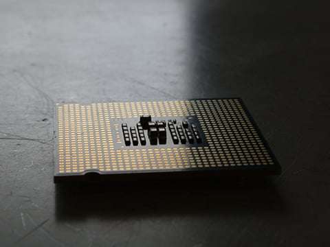
In traditional microelectronics, sputtered aluminum has long been used for interconnects, contact pads, and wiring layers on silicon wafers. These films carry signals and power across the chip and must combine low resistivity with good patterning behavior.
Even as some advanced nodes move to copper or other metals, aluminum remains important in mature processes, power devices, MEMS, and analog circuits, where stability, process familiarity, and cost control are key. Here, consistent aluminum target purity and grain structure help keep line resistance and electromigration performance within tight limits.
Display and Optoelectronic Devices

In displays, aluminum thin films are used in backplane structures, driver circuits, and reflective layers. For example, aluminum can serve as a back reflector in LCD or OLED modules to improve brightness and energy efficiency. It may also appear in sensor pixels, light shields, or signal lines around the active area.
Because displays often involve large-area coating, aluminum sputtering targets must support uniform deposition over wide substrates, with reliable film thickness and low particle levels.
Solar and Energy-Related Coatings

Crystalline silicon solar cells commonly use aluminum on the rear side as an electrode and reflector. This thin aluminum layer helps extract current while reflecting unabsorbed light back into the absorber layer to increase efficiency. In some thin-film PV designs, aluminum is also used in bus bars, contact layers, or reflective stacks.
For these applications, aluminum targets need to offer good conductivity and reflectivity, but also stable behavior in high-throughput production, where target life and utilization directly affect cost.
Optical Components and Sensor Systems

Optical instruments, sensors, and scientific equipment often rely on aluminum mirrors and reflective coatings. Sputtered aluminum provides strong reflectance in the visible and near-infrared range and can be combined with protective overcoats to improve durability.
In these systems, surface quality is critical. A dense, smooth film produced from a high-quality aluminum target helps achieve the required optical performance with minimal scattering or distortion.
Packaging and Flexible Electronics

In flexible electronics, barrier films, and advanced packaging, thin aluminum layers are used to block moisture, oxygen, or light. These coatings help protect OLED panels, flexible displays, and sensitive electronic modules while keeping the structure light and bendable.
Here, adhesion, mechanical stability, and controlled thickness are just as important as conductivity. Choosing the right aluminum sputtering target and process conditions helps ensure the film can withstand bending, lamination, and long-term environmental exposure.
In the next section, you can move naturally into why sputtering is the preferred deposition method for these aluminum films and how the choice of target ties into process performance.
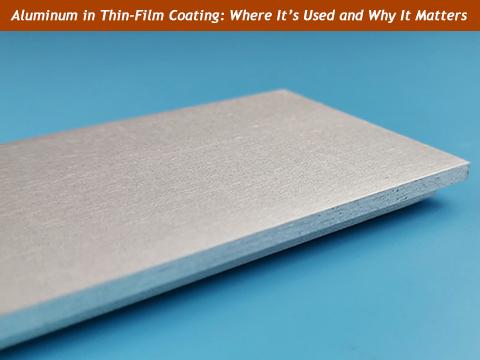
Choosing the Right Aluminum Sputtering Target for Your Process
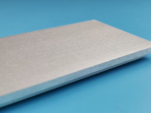
No matter how advanced your coating system is, the quality of the thin film starts with the sputtering target itself. In the case of aluminum, selecting the right target isn’t just about choosing a metal — it’s about aligning purity, grain structure, size, bonding, and even alloying with the demands of your process.
Purity Grades and Their Impact
Aluminum sputtering targets are available in various purity levels, typically ranging from 99.9% (3N) up to 99.999% (5N). The correct grade depends on your application:
- 5N aluminum targets are ideal for semiconductor metallization, optical films, and high-reliability electronics, where even trace impurities can affect conductivity or cause film defects.
- 4N targets are commonly used in display panels, solar cell coatings, and general-purpose PVD applications, offering a good balance of purity and cost.
- 3N targets may be suitable for barrier layers or less demanding industrial coatings where ultra-low impurity levels aren’t critical.
The higher the purity, the more stable the film characteristics tend to be — including electrical resistivity, reflectivity, and particle suppression during deposition.
Target Geometry: Planar vs. Rotary
Depending on your sputtering system, you may need planar aluminum targets or rotary (cylindrical) targets.
- Planar targets are widely used in batch tools and R&D systems. They are easy to install, cost-effective, and support precise layer-by-layer deposition.
- Rotary targets are preferred in large-area coating systems or inline production tools. They offer longer target life, higher material utilization, and fewer shutdowns — especially important in high-throughput environments like solar panel or display production.
Choosing the right geometry helps reduce downtime, improve coating uniformity, and lower long-term production costs.
Alloyed Aluminum Targets for Specific Needs
While pure aluminum is widely used, certain applications benefit from alloyed targets such as:
- Aluminum-Copper (Al-Cu): Improves electromigration resistance in semiconductor interconnects.
- Aluminum-Silicon (Al-Si): Common in TFT-LCD backplanes for improved film adhesion and stability.
- Aluminum-Neodymium (Al-Nd): Enhances hardness and oxidation resistance in optical or structural films.
We offer a full range of aluminum alloy sputtering targets, with customizable dopant levels and verified composition using XRF and ICP-MS analysis.
At AEM Deposition, we provide aluminum sputtering targets with customizable specs, bonded or unbonded formats, and tight purity control — all backed by material certification and fast export support. Whether you’re working in R&D or mass production, our engineering team can help you source the right target for your coating line.
Conclusion
Aluminum remains one of the most widely used materials in thin-film coating—valued for its conductivity, reflectivity, and cost-effectiveness. From semiconductors and displays to solar cells and optical systems, aluminum thin films serve multiple roles in modern devices. And across each of these industries, sputtering stands out as the preferred method for achieving stable, high-quality aluminum coatings.
Choosing the right aluminum sputtering target is critical to film performance. Factors like purity level, target design, and alloy composition directly impact coating results and long-term reliability. Whether you're developing a new display product or optimizing large-scale PV production, starting with the right target makes the difference.
At AEM Deposition, we supply high-purity aluminum sputtering targets in a wide range of sizes, grades, and custom alloy options. From R&D labs to full-scale fabs, our materials support consistent performance and scalable results.
Need a quote or expert guidance? Contact our team to get application-specific advice or request pricing for your next project. Let’s build your next thin-film solution with confidence.