


 +86-731-89578196
 [email protected]

- Home
- Our Company
-
Products
Sputtering Targets

- Industries
- Blog
- FAQ
- Contact Us


Copper Sputtering Targets: High-Performance Solutions for Thin Film Deposition
views, Updated: 2025-12-12
Introduction
Thin-film deposition is an important process used to create the coatings found in many modern technologies, from electronics to solar panels. One of the most common ways to do this is through sputtering, a process where atoms are blasted off a target material and deposited onto a surface to form a thin, even layer.
Copper is one of the most popular materials used for sputtering targets. It’s used in industries like electronics, solar energy, and optics because it has great electrical conductivity, heat resistance, and durability. These qualities make copper perfect for creating high-performance thin films.
Copper sputtering targets are essential for making things like microchips, improving solar panel efficiency, and creating thin coatings for optical devices. Copper is a great choice because it’s cost-effective, long-lasting, and performs well in many different applications.
In this article, we’ll explain what copper sputtering targets are, why they’re so important, and where they’re used. We’ll also guide you on how to choose the right copper target for your needs and give you a look at how these targets are made.
1. What is a Copper Sputtering Target?
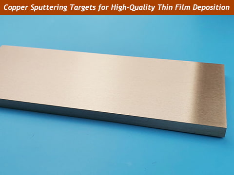
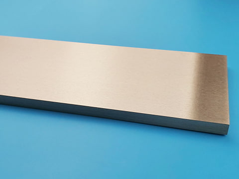
A copper sputtering target is a high-purity copper material used in the sputtering process to deposit thin films of copper onto various substrates. Sputtering is a widely used technique in thin-film deposition, particularly in the semiconductor, electronics, and materials science industries. It involves bombarding a target material (in this case, copper) with high-energy ions, which causes atoms from the target to be ejected and deposited onto the surface of a substrate.
In the context of copper sputtering targets, the target material is typically a disc or a cylindrical shape made from copper metal. These targets serve as the source of copper atoms that are transferred onto substrates in a vacuum chamber. The sputtered copper atoms then condense onto the surface, forming a thin, uniform copper film.
How Sputtering Works
The sputtering process begins when an inert gas, often argon, is introduced into the vacuum chamber. The gas is ionized by applying a high voltage to the chamber, which accelerates the ions towards the copper target. When these ions collide with the target, they cause copper atoms to dislodge and be ejected onto the substrate surface. The copper atoms then form a thin film on the substrate, which can be used in the manufacturing of a wide range of products, from microelectronics to solar cells.Why Copper?
Copper is chosen for sputtering due to its excellent electrical and thermal conductivity, as well as its high resistance to corrosion. These properties make copper an ideal material for creating thin films used in high-performance electronic devices, semiconductors, and energy systems.Common applications of copper sputtering targets include:
- Semiconductors: Copper is used in the deposition of interconnects, vias, and microchip components, providing excellent electrical conductivity for electronic devices.
- Solar Panels: Copper thin films are used in photovoltaic cells, where they help improve the efficiency of energy conversion.
- Optical Coatings: Copper is used for creating thin films in optical devices such as mirrors and lenses.
2. Key Properties of Copper for Sputtering Applications
Copper is a top choice for sputtering targets because of its combination of useful properties that make it perfect for a wide range of applications. Let’s dive into why copper is so effective in the sputtering process.
Electrical Conductivity
One of copper's most important features is its excellent electrical conductivity. Copper allows electricity to flow easily, which is why it’s widely used in electronics. When used in sputtering, it forms thin films that act as the conductive paths in circuit boards, microchips, and other electronic components—ensuring they work efficiently and reliably.Thermal Conductivity
Copper also has great thermal conductivity, meaning it’s really good at transferring heat. This is crucial for applications like power electronics and semiconductors, where keeping components cool is vital. Copper helps dissipate heat quickly, preventing overheating and ensuring better performance over time.Malleability and Ductility
Copper is both malleable and ductile, which means it can be easily shaped and stretched without breaking. This flexibility makes it ideal for creating thin films with intricate designs. Whether it’s forming precise layers on a microchip or creating flexible electronic components, copper can be molded into the exact shape needed for the job.Corrosion Resistance
Another reason copper is favored is its natural resistance to corrosion. Unlike many other metals, copper doesn’t rust or degrade easily, even when exposed to the elements. This is particularly important in applications like solar energy, where the thin films need to endure outdoor conditions and maintain their performance over time.High Purity
Copper used for sputtering is often of very high purity (usually 99.9% or higher). This ensures that the thin films deposited are clean and free from contaminants, which is essential in industries like semiconductors, where even the smallest impurity can affect the performance of the final product.Cost-Effectiveness
Finally, copper is affordable compared to other high-conductivity metals like silver and gold. Despite being cheaper, it still performs exceptionally well in sputtering processes, making it a great choice for large-scale production in industries that need to keep costs in check without compromising on quality.3. Applications of Copper Sputtering Targets
Copper sputtering targets are used in a wide variety of industries due to their excellent properties. Their ability to create high-quality, durable thin films makes them essential for many high-tech applications. Here are some of the key areas where copper sputtering targets play a critical role.
Semiconductors
One of the biggest uses of copper sputtering targets is in the semiconductor industry. Copper is used to create thin films for interconnects, vias, and microchip components. It’s essential for forming the electrical pathways that connect different parts of a chip. With its excellent conductivity, copper helps ensure that chips function efficiently and reliably. The move towards copper interconnects in semiconductors has been driven by the need for faster, more energy-efficient devices.Solar Panels
Copper sputtering targets are also widely used in the solar energy industry, particularly for photovoltaic cells. Copper thin films help increase the efficiency of solar panels by improving electrical conductivity and energy conversion. Copper is an ideal material for these applications because of its durability, corrosion resistance, and ability to perform in outdoor conditions. By using copper sputtering targets, manufacturers can create high-quality, efficient solar panels that can stand up to the elements for years.Optical Coatings
Copper sputtering is essential in the optics industry for creating reflective coatings on mirrors, lenses, and other optical components. Copper thin films help improve the performance of these devices by providing high reflectivity and durability. These coatings are used in a wide range of applications, from telescopes and cameras to laser systems and microscopes. Copper’s ability to create uniform and stable films makes it an excellent choice for high-performance optical devices.Magnetic Materials
In the magnetic materials industry, copper sputtering targets are used to create thin films for memory devices, data storage, and other magnetic applications. Copper’s excellent electrical and thermal properties make it ideal for producing magnetic films that are both stable and efficient. These thin films are used in a variety of devices, from hard drives to advanced sensors.Wiring and Conductors
Copper is well-known for its high electrical conductivity, which makes it a natural choice for use in wiring and conductive applications. Copper sputtering targets are used to create thin, flexible copper films for use in flexible electronics, wearable devices, and printed circuit boards (PCBs). These thin films help ensure that electrical signals travel quickly and efficiently, which is crucial for modern electronic devices.Decorative Coatings
Copper sputtering targets are also used for decorative coatings. Copper’s natural color and luster make it a popular choice for creating visually appealing finishes on a variety of products. From automotive parts to jewelry and architectural features, copper thin films offer a durable, attractive solution that resists tarnishing and corrosion.Batteries and Energy Storage
Copper sputtering targets are used in the manufacture of electrodes for batteries and supercapacitors. Copper’s high conductivity ensures that energy storage devices operate efficiently, providing reliable power for everything from smartphones to electric vehicles. Thin copper films can enhance the performance and lifespan of these energy storage systems, making them more effective for long-term use.LEDs and Lighting
In the LED and lighting industries, copper sputtering targets are used to create thin films for high-efficiency light-emitting diodes (LEDs). Copper’s ability to conduct heat and electricity efficiently helps improve the performance and longevity of LED lights. It’s also used in creating the conductive layers in OLED displays, which are found in everything from smartphones to large-screen televisions.4. The Common Copper Alloy Sputtering Targets
While pure copper is commonly used in sputtering, copper alloys are also popular choices for specific applications. Copper alloys combine copper with other metals to improve certain properties like strength, hardness, corrosion resistance, or specific electronic characteristics. These alloys offer unique benefits, making them suitable for a wide range of industries and applications.
Let’s explore some of the most common copper alloy sputtering targets and how they are used.
1. Copper-Nickel (Cu-Ni) Alloy Sputtering Targets
Copper-nickel alloys are commonly used for sputtering in industries that require enhanced corrosion resistance and improved mechanical properties.- Properties: Copper-nickel alloys offer better resistance to corrosion than pure copper, especially in environments exposed to seawater or harsh chemicals. They also have good thermal and electrical conductivity.
- Applications: These alloys are widely used in the electronics industry, particularly for interconnects, thin-film resistors, and varistors. They are also used in marine and chemical industries due to their resistance to corrosion.
2. Copper-Tin (Cu-Sn) Alloy Sputtering Targets
Copper-tin alloys are known for their hardness and wear resistance, which makes them ideal for applications where durability and strength are important.- Properties: The addition of tin to copper increases the material's hardness, making it more resistant to wear and tear. These alloys are also commonly used in situations where oxidation resistance is important.
- Applications: Copper-tin alloy sputtering targets are often used in automotive, aerospace, and industrial coatings. They are also found in electrical contacts and bearings, where high strength and corrosion resistance are critical.
3. Copper-Zirconium (Cu-Zr) Alloy Sputtering Targets
Copper-zirconium alloys are often used for high-performance applications that require a combination of excellent conductivity and high thermal stability.- Properties: Copper-zirconium alloys offer improved hardness and thermal resistance over pure copper. The addition of zirconium increases the material's resistance to high temperatures, making it suitable for demanding environments.
- Applications: These alloys are frequently used in electrical components that need to endure high temperatures, such as power generation equipment, electrical contacts, and high-voltage applications. They are also used in aerospace and nuclear industries where high thermal stability is required.
4. Copper-Chromium (Cu-Cr) Alloy Sputtering Targets
Copper-chromium alloys are known for their excellent strength and conductivity properties, particularly at high temperatures.- Properties: Copper-chromium alloys are resistant to oxidation and wear, which makes them ideal for environments with high temperatures or electrical currents. The chromium content increases the material’s hardness while maintaining good electrical and thermal conductivity.
- Applications: These alloys are used in electrical contacts, welding, and high-temperature applications like arc welding or electrical conductors. They are also used in automotive and industrial machinery components that require resistance to heat and wear.
5. Copper-Aluminum (Cu-Al) Alloy Sputtering Targets
Copper-aluminum alloys combine the high strength of aluminum with the conductivity of copper, making them a good choice for certain types of thin films.- Properties: These alloys offer high strength and resistance to corrosion, particularly in environments where aluminum’s properties are needed. Copper-aluminum alloys also maintain a balance between conductivity and mechanical strength.
- Applications: These alloys are used in automotive parts, aerospace components, and structural applications. They are also found in electronics that require a mix of strength, durability, and conductivity.
6. Choosing the Right Copper Sputtering Target for Your Process
Selecting the right copper sputtering target is essential for achieving high-quality thin films that meet your specific requirements. The target you choose affects the performance, stability, and efficiency of the sputtering process, whether you’re working in semiconductors, solar energy, or electronics. Here are the key factors to consider when choosing a copper sputtering target.
1. Purity of the Copper Target
The purity of the copper target plays a critical role in the quality of the thin films. Copper targets with a purity of 99.999% are commonly used in sputtering because they have very low levels of impurities, which can affect the film’s performance.- Why Purity Matters: Higher purity copper ensures better electrical conductivity and film stability, which are crucial for applications like semiconductors and solar cells. Fewer impurities mean fewer defects in the thin film, leading to better performance and reliability.
- Impact on Film Quality: Even the smallest impurities can affect the thin film's conductivity and stability. By choosing high-purity copper, you reduce the risk of contamination during sputtering, leading to a smoother and more uniform film.
2. Grain Structure of the Copper Target
The grain structure of the copper target is just as important as its purity. A uniform grain structure ensures that the sputtered copper atoms deposit evenly on the substrate, which is essential for producing consistent and high-quality thin films.- Why Grain Structure Matters: If the grain structure is uneven, it can cause non-uniform film thickness, leading to poor performance. This is especially critical in industries like semiconductors, where uniform layers are essential for the functionality of the final product.
3. Size and Shape of the Copper Target
The size and shape of the copper target must match the requirements of your sputtering system and the substrate you’re working with.- Target Size: Larger targets are used for high-volume production, while smaller ones are suitable for research or smaller-scale applications. Choose a target size that fits your sputtering system and production needs.
- Target Shape: Copper sputtering targets are typically available in round, rectangular, or custom shapes. The shape should match your sputtering system’s cathode and the type of substrate you’re coating.
4. Copper Alloy (If Needed)
If your application requires specific properties, you might choose a copper alloy sputtering target. Alloys like copper-nickel or copper-zirconium offer enhanced corrosion resistance, strength, or thermal stability.- When to Use Alloys: Copper alloys are used when you need improved performance in specific conditions, such as better resistance to heat or wear. For example, copper-nickel alloys are excellent for corrosion-resistant applications, while copper-zirconium alloys are used for high-temperature environments.
5. Deposition Rate and Efficiency
The deposition rate is the speed at which the copper atoms are deposited onto the substrate. This rate is influenced by the power settings, pressure, and distance in your sputtering system.- Optimizing Deposition Rate: A higher deposition rate can speed up the process, but it may also lead to less uniform films. It’s important to balance speed and film quality. For high-volume production, you may need a faster deposition rate, but for precision applications, a slower rate might be better to ensure uniformity and stability.
6. Consider Your Specific Application
Your choice of copper sputtering target will depend on the specific needs of your application. For instance:- Semiconductors need thin films with excellent electrical properties and uniformity.
- Solar panels require copper films that maximize conductivity and energy conversion efficiency.
- Optical coatings benefit from copper's reflective properties and resistance to corrosion.
7. Copper Sputtering Target Manufacturing Process
The manufacturing process of copper sputtering targets is a multi-step procedure that ensures high-quality targets with excellent performance characteristics, such as low oxygen content, high density, and fine, uniform grain size. Below is an overview of how high-purity copper sputtering targets are produced.
1. Raw Material Selection and Electrolytic Refining
The process begins with the use of ordinary electrolytic copper as the raw material. This copper undergoes a series of purification steps to achieve high purity, which is critical for the sputtering process.- Electrolytic Refining: The copper is first purified through electrolytic refining, which removes impurities and enhances the material's overall purity. This ensures that the final copper target has very low levels of contaminants that could affect the quality of the thin films produced during sputtering.
2. Vacuum Induction Melting and Electron Beam Melting
Once the copper is refined, it is subjected to vacuum induction melting (VIM) and vacuum electron beam melting (EBM). These processes are essential for producing copper ingots with extremely low oxygen content and ensuring a high level of material purity.- Vacuum Induction Melting (VIM): This step involves melting the copper in a vacuum, which helps eliminate any remaining oxygen or impurities.
- Electron Beam Melting (EBM): The copper is further melted using an electron beam in a controlled vacuum environment, which helps achieve high-density, oxygen-free ingots that are the foundation for high-performance sputtering targets.
3. Hot Forging and Heat Treatment
After the copper ingot is formed, it undergoes several cycles of hot forging and heat treatment to refine the material and improve its mechanical properties.- Hot Forging: The ingot is heated and then subjected to mechanical pressure to shape it into the desired size and form, reducing its grain size and improving the overall structure of the copper.
- Heat Treatment: The copper is then heat-treated to further refine its properties, relieve internal stresses, and enhance its ductility and malleability.
4. Cold Forging and Heat Treatment
Once the copper has been hot-forged and treated, it goes through a cycle of cold forging and subsequent heat treatment to ensure the material achieves the right combination of hardness and flexibility.- Cold Forging: This process helps achieve further refinement of the copper’s grain structure and enhances the material’s strength without affecting its inherent conductivity.
- Heat Treatment: The material undergoes additional heat treatment to ensure uniform properties throughout the copper and to prepare it for the final rolling and shaping steps.
5. Hot Rolling and Cold Rolling
The copper undergoes both hot rolling and cold rolling to achieve the correct dimensions and further improve its properties.- Hot Rolling: The copper is rolled at high temperatures, which helps reduce its thickness and improve its homogeneity.
- Cold Rolling: After hot rolling, the copper is subjected to cold rolling, which helps increase its strength and refine its surface texture.
6. Final Heat Treatment
After rolling, the copper is once again subjected to heat treatment to optimize its final structure. This step ensures that the copper has the right balance of hardness and flexibility, preparing it for the final machining and polishing stages.7. Mechanical Processing, Grinding, and Polishing
At this stage, the copper target is ready for mechanical processing. This includes precision grinding and polishing to give the sputtering target its final shape and smooth surface.- Grinding and Polishing: These final steps ensure that the copper sputtering target is free from surface defects and has the required finish for sputtering. The target is ground to exact specifications and polished to a high shine, ready for use in thin-film deposition applications.
8. Quality Control and Testing
Throughout the entire manufacturing process, the copper sputtering target undergoes rigorous quality control and testing to ensure that it meets strict standards for:- Oxygen Content: The final copper target must have an oxygen content of ≤10 ppm to ensure high conductivity and uniform thin film deposition.
- Grain Size: The copper target’s grain size is controlled to ensure it remains ≤50μm, which is essential for achieving a uniform, high-quality film.
Conclusion
Copper sputtering targets are a key material for creating high-quality thin films used in industries like electronics, solar energy, and optics. Copper is a great choice because it offers good conductivity, durability, and is cost-effective.
When you purchase copper sputtering targets, you’re ensuring that your thin films will be consistent, stable, and have the right electrical properties for your products to work well. Copper targets with high purity (99.999%) are especially important for better performance and fewer defects in your films.
To make the best purchase, consider factors like purity, grain structure, and target size. These factors will help you choose the right copper sputtering target for your specific needs, whether it’s for microchips, solar panels, or optical coatings.
If you’re unsure which copper sputtering target is best for your process, we’re here to help. Our team can guide you in making the right choice, so you get the best performance and value for your investment.
LATEST NEWS