


 +86-731-89578196
 [email protected]

- Home
- Our Company
-
Products
Sputtering Targets

- Industries
- Blog
- FAQ
- Contact Us


Enhance Your Sputtering Deposition Performance with Cutting-Edge Sputtering Targets
Understanding Sputtering Deposition
In the realm of thin-film deposition techniques, sputtering is a process that stands out for its versatility and efficiency. It involves the removal of atoms from a solid target material through bombardment with energetic particles, typically ions or neutral atoms. This process creates a thin film on a substrate, a fundamental principle behind many modern technological innovations.
Definition and Basic Principles of Sputtering Deposition
Sputtering deposition is based on the concept of momentum transfer. When energetic particles collide with the target material, they transfer their momentum to the target atoms, causing them to be ejected. These ejected atoms then travel to the substrate and form a thin film. This process can be performed in a vacuum environment to avoid contamination and to ensure the purity of the deposited film.
Types of Sputtering Deposition
There are several types of sputtering techniques, including DC sputtering, RF sputtering, and magnetron sputtering. Each technique has its own advantages and is suited to different applications.
- DC Sputtering: Direct current (DC) sputtering is a simple and cost-effective method that uses a constant voltage to create a plasma. It is often used for deposition of metals and metallic compounds.
- RF Sputtering: Radio frequency (RF) sputtering uses an RF power source to create a high-energy plasma, allowing for a more controlled and uniform deposition process. This technique is commonly used for dielectric materials.
- Magnetron Sputtering: Magnetron sputtering uses magnetic fields to enhance the plasma density near the target surface, leading to higher deposition rates and improved film quality. It is widely used in the production of thin films for various applications.
Key Applications in Various Industries
Sputtering deposition has found widespread use in a variety of industries due to its ability to deposit high-quality thin films with precise control over thickness and composition.
- Electronics: In the electronics industry, sputtering is used to deposit thin films for integrated circuits, flat panel displays, and magnetic storage media.
- Solar Energy: Sputtering is used to manufacture thin-film solar cells, which offer a cost-effective alternative to traditional silicon-based solar panels.
- Automotive: Sputtering is used to deposit thin films on automotive glass for improved durability, UV protection, and heat insulation.
Advantages of Sputtering Deposition over Other Thin-Film Techniques
Compared to other thin-film deposition techniques such as evaporation and chemical vapor deposition (CVD), sputtering offers several advantages:
- Uniformity: Sputtering provides excellent film uniformity, making it ideal for applications where precise control over film thickness and composition is required.
- Versatility: Sputtering can be used to deposit a wide range of materials, including metals, semiconductors, and insulators, making it suitable for a variety of applications.
- Efficiency: Sputtering has a high material utilization rate, minimizing waste and reducing production costs.
In conclusion, sputtering deposition is a versatile and efficient thin-film deposition technique with a wide range of applications across various industries. Its ability to deposit high-quality films with precise control makes it an essential technology in the manufacturing of advanced electronic, solar energy, and automotive products.
The Sputtering Deposition Process
Sputtering deposition is a complex yet fascinating process that plays a crucial role in the production of thin films for various applications. Understanding the intricacies of this process can provide valuable insights into its efficiency and effectiveness.
Detailed Explanation of the Sputtering Deposition Process
The sputtering deposition process begins with the creation of a plasma, a state of matter in which atoms are ionized and form a highly reactive gas. This plasma is typically created by applying a high voltage or radio frequency (RF) power to a gas, such as argon, in a vacuum chamber.
Once the plasma is established, energetic ions in the plasma are accelerated towards a solid target material. When these ions strike the target, they transfer their kinetic energy to the target atoms, causing them to be ejected from the surface. These ejected atoms then travel to the substrate, which is positioned facing the target, and deposit onto its surface, forming a thin film.
Vacuum Environment
The sputtering deposition process is typically performed in a vacuum environment to prevent contamination and ensure the purity of the deposited film. A vacuum chamber is used to create and maintain the required low-pressure environment, typically in the range of 10-3 to 10-6 torr.
Target Material Interaction with Plasma
The target material plays a critical role in the sputtering process. It must be selected based on the desired properties of the thin film. When the energetic ions in the plasma collide with the target material, they cause the ejection of target atoms. The composition of the target material determines the composition of the deposited film.
Film Formation on the Substrate
As the ejected target atoms travel to the substrate, they form a thin film on its surface. The film thickness and uniformity are controlled by factors such as the sputtering time, the distance between the target and the substrate, and the rate of deposition.
Factors Influencing the Deposition Process
Several factors can influence the sputtering deposition process, including:
- Pressure: The pressure of the gas in the vacuum chamber affects the mean free path of the ions and, consequently, the efficiency of the sputtering process.
- Power: The power applied to the plasma determines the energy of the ions and, therefore, the rate of sputtering and deposition.
- Substrate Temperature: The temperature of the substrate can affect the adhesion and crystalline structure of the deposited film.
In conclusion, the sputtering deposition process is a highly controlled and versatile technique for depositing thin films with precise control over thickness, composition, and structure. By understanding the intricacies of this process, researchers and engineers can harness its potential for a wide range of applications in electronics, optics, and materials science.
The Role of Sputtering Targets in Deposition
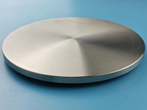
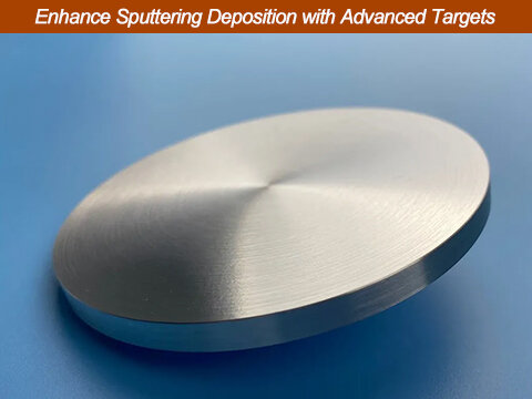
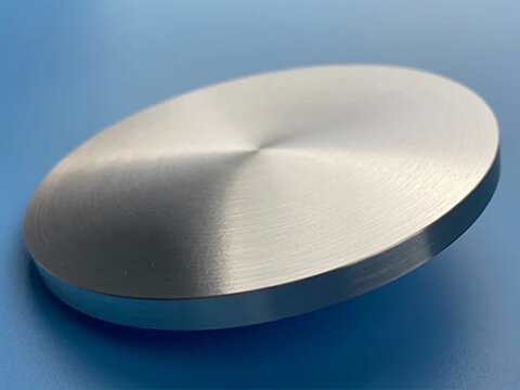
Sputtering targets are essential in creating thin films through sputtering deposition. They are solid materials, like metals, alloys, or ceramics, that serve as the source for thin film atoms.
What are Sputtering Targets?
Sputtering targets are solid materials used as the source of atoms for thin film deposition in sputtering processes. They are made from metals, alloys, or ceramics, chosen based on the desired properties of the thin film.
Materials Used in Sputtering Targets
Sputtering targets can be made from metals like aluminum and copper, alloys like titanium-aluminum, or ceramics like silicon dioxide. Each material is chosen for specific properties needed in the thin film.
How Sputtering Targets Impact Thin Film Quality and Properties
The choice of sputtering target material affects the quality and properties of the thin films produced.
- Composition: The target material's composition determines the composition of the deposited thin film, impacting properties like conductivity or hardness.
- Purity: Target material purity is crucial for ensuring high-quality thin films. Even tiny impurities can affect film properties.
- Microstructure: The target material's microstructure can influence the deposited thin film's microstructure, affecting its mechanical and optical properties.
In conclusion, sputtering targets are critical for controlling thin film properties. By selecting the right target material, researchers and engineers can achieve precise control over thin film deposition for various applications.
Benefits of Premium Sputtering Targets
Premium sputtering targets offer significant advantages over standard targets, improving thin film deposition processes in several key ways:
- Uniformity and Adhesion: Premium targets provide better film uniformity and adhesion, resulting in more durable coatings.
- Deposition Rates and Efficiency: They offer higher deposition rates, leading to faster production and increased efficiency.
- Reduced Impurities and Defects: Premium targets are made with high-purity materials, reducing impurities and defects in the thin film.
- Longer Lifespan and Cost-Efficiency: They have a longer lifespan, reducing downtime and maintenance costs.
- Consistency: Premium targets undergo strict quality control, ensuring consistent performance and better quality thin films.
In conclusion, using premium sputtering targets can optimize thin film manufacturing processes, leading to higher-quality coatings and improved efficiency.
Selecting the Right Sputtering Targets for Optimal Deposition
Choosing the correct sputtering targets is critical for achieving ideal thin film deposition. Consider factors such as material composition, size, purity, and compatibility with the deposition system. Customization options are available for specific application needs. Work with reliable suppliers to ensure quality assurance and technical support. For premium sputtering targets tailored to your needs, work with our company: AEM Deposition.
Future Trends in Sputtering Deposition and Target Technology
Discover the latest trends in thin-film technology. New sputtering targets, like graphene and complex metal oxides, are improving semiconductors and solar cells. High-power impulse magnetron sputtering (HiPIMS) and reactive sputtering make better quality films faster. Expect more advances for electronics, energy, and healthcare, including flexible screens, sensors, and solar cells.