+86-731-89578196
 [email protected]

- Home
- Our Company
-
Products
Sputtering Targets

- Industries
- Blog
- FAQ
- Contact Us


DC Sputtering VS RF Sputtering
views, Updated: 2022-12-16
What is Sputtering:Sputtering is a vacuum deposition technique used to deposit thin-film of a material onto a surface.
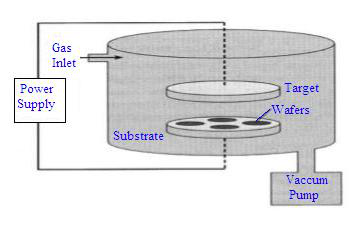
The substrates are placed into the vacuum chamber and pumped down to process pressure. First, creating gaseous plasma accelerates the ions from this plasma into some source material. It is used to knock atoms out of the target. The molecules, atoms, ions, and electrons on the target's surface are sputtered out in the process.
The emitted particles have a certain kinetic energy and are directed toward the substrates' outer surface in a particular direction to deposit on the surface of the substrate. The higher pressure can help to generate better coverage. The excess energy of metal ions can increase surface mobility in the sputtering process.
DC Sputtering:
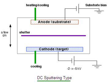
• The power source is the Direct Current (DC) type.
• Chamber pressure is usually from 1 to 100 mTorr
• DC power is usually preferred for electrically conductive target materials as it’s effective and economical. Such as pure metal sputtering targets, Iron (Fe), Copper (Cu), Nickel (Ni).
• It is a simple technique when processing large quantities of large substrates.
• The deposition rate is high for some pure metal sputtering targets
• The positively charged sputtering gas is accelerated towards the target in DC sputtering, and the ejection of atoms gets deposited on substrates.
RF Sputtering:
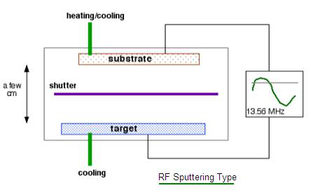
• The power source is AC (Alternating Current). The power supply is a high voltage RF source often fixed at 13.56 MHz.
• RF peak to peak voltage is 1000 V, electron densities are 109 to 1011 Cm-3, and the chamber pressure is from 0.5 to 10 mTorr.
• RF sputtering has a wider range of applications and is suitable for all the materials for conductive and non-conductive materials. However, it is most commonly used for depositing dielectric sputtering target materials.
• The deposition rate is lower compare with DC sputtering.
• It is used for smaller substrate sizes due to the high cost.
• The RF sputtering involves two processes. In the first cycle, the target material is negatively charged. This results in atoms' polarization, and the sputtering gas atoms are attracted to the source, where they knock outsource atoms.
Due to polarization, the source atoms and ionized gas ions remain on the target surface.
• In the second cycle, the target is positively charged. Due to reverse polarization, this causes the ejection of gas ions and source atoms. These ions and atoms accelerated toward the substrate to form deposition.
Following table summarizes difference between RF sputtering and DC sputtering
| Features | DC Sputtering | RF Sputtering |
| Sputtering Type | Magnetron only | Magnetron or diode |
| Target Materials | Conductive only | All the targets (conductive and non-conductive materials) |
| Sputtering Rate | 100% of DC | 20% of DC, no magnetron |
| Cost and Complexity | Best | Expensive and complex than DC sputtering |
| Campaign Length (i.e. loss of anode) | Good | Excellent |
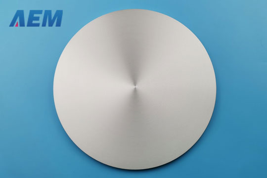
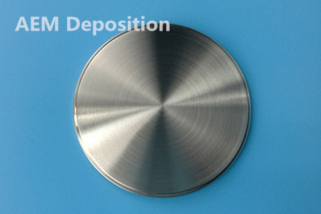
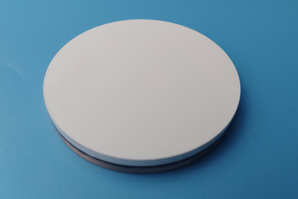
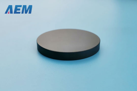
AEM Deposition provides various sputtering targets (Pure metal sputtering targets, Oxide sputtering targets, Sulfide sputtering targets) suitable for DC & RF sputtering.
LATEST NEWS