Sputtering Targets
Evaporation Materials
Evaporation Sources
High Purity Materials
Thin Film Substrates
Crytstal Materials


 +86-731-89578196
 [email protected]
Sputtering Targets

At AEM, we pride ourselves on being a leading silicon wafer supplier, known for our commitment to precision and performance. With years of experience in the semiconductor industry, we provide high-quality silicon wafers that meet the strictest industry standards.
By choosing AEM, you gain a reliable partner dedicated to meeting your specific needs with tailored wafer solutions. Our team is focused on quality, innovation, and customer satisfaction, providing you with wafers that drive technological advancement and reliability.
| Grade | Prime, Test, Dummy |
|---|---|
| Size | 10x10, 15x15, 20x 15, 20x 20 (customized sizes are available),Dia 1'', Dia 2'',Dia 3'', Dia 4'', Dia 5'' Dia 6'', Dia 8''. Dia12'' |
| Thickness | 0.3- 0.5mm, 1.0mm |
| Polished | SSP or DSP |
| Orientation | <100>,<110>, <111> |
| Redirection Precision | ±0.5° |
| Redirection the Edge | 2°(special in 1°) |
| Material | Silicon | ||
|---|---|---|---|
| Growth Method | CZ, MCZ, FZ | ||
| Structure | M3 | ||
| Melting Point | 1420℃ | ||
| Density(g/cm3) | 2.4 g/cm3 | ||
| Doped Material | undoped | B-doped | P-doped |
| Type | P /N | P | N |
| Resistivity | >1000 Ωcm | 10-3 ~40 Ωcm | 0.05~0.1 Ωcm |
| Thermal-expans | ≤100/cm2 | ≤100/cm2 | ≤100/cm2 |
Our silicon wafers are produced using advanced technology, ensuring exceptional purity and uniformity for consistent performance in critical applications.
We employ cutting-edge techniques to achieve precise specifications, meeting the highest industry standards for reliability and accuracy.
We offer a range of wafer sizes and specifications tailored to your specific needs, providing flexible solutions for diverse applications.
Each wafer undergoes thorough testing to guarantee durability and performance, ensuring you receive a product that meets your highest expectations.
Our knowledgeable team is dedicated to providing personalized support and guidance, helping you choose the best wafers for your projects.
Silicon is extracted from sand, primarily composed of silicon dioxide. The sand is mixed with carbon and melted at temperatures above 2000°C to separate silicon from impurities. The result is a silicon product that is about 99% pure. To achieve higher purity, the silicon is ground into a fine powder and processed in a Fluidized Bed Reactor (FBR) with hydrochloric acid at around 300°C. This process, followed by distillation, yields silicon with a purity of 99.9999%.
The silicon boule is cut into manageable lengths, which are then ground to the desired diameter, ranging from 100 mm to 450 mm. Wafers with diameters under 200 mm have orientation flats added to indicate crystal axes and doping types. For larger wafers, a single groove along the crystal axis indicates the orientation.
Wafers are sliced from the ingot using diamond blades or multi-wire saws. Diamond blades cut each wafer individually, resulting in smoother surfaces but lower productivity. Multi-wire saws, coated with diamond particles and running at high speeds, cut multiple wafers simultaneously, although this method results in rougher surfaces that require additional processing.
After slicing, wafers undergo chamfering to round their sharp edges and prevent cracking. Grinding follows to remove saw marks and surface imperfections, enhancing the wafer's flatness, curvature, and parallelism. This step ensures the wafers meet technical requirements for further processing.
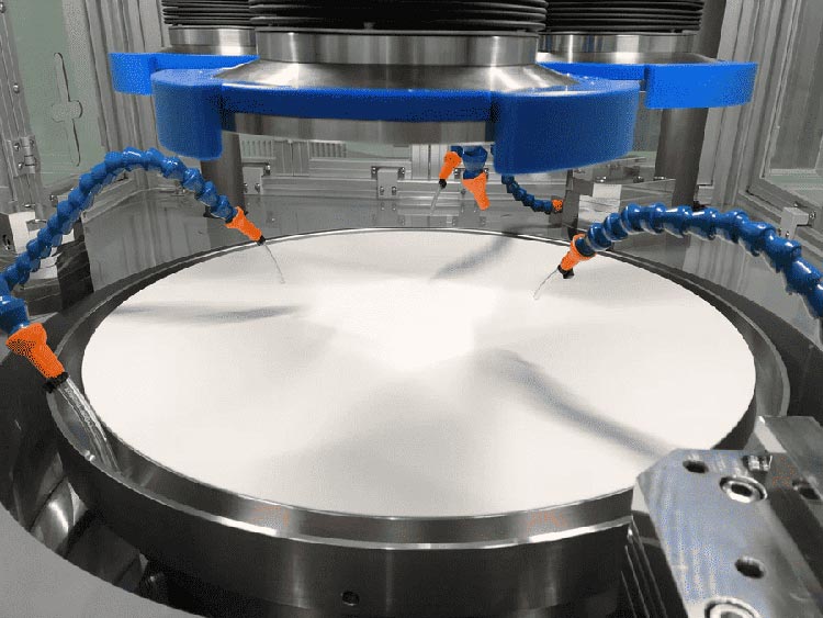
To remove damaged surface layers, wafers are etched using solutions like potassium hydroxide (KOH) or a combination of nitric acid and hydrofluoric acid. Following etching, wafers undergo chemical-mechanical polishing (CMP) to achieve a high-reflectivity, mirror-like surface. This process involves using a polishing pad and a slurry of abrasive particles to remove any remaining surface defects.
Cleaning is a crucial step, involving the removal of particles, organic, and inorganic contaminants. Wafers are cleaned using traditional RCA procedures with hydrogen peroxide and ammonium hydroxide, as well as advanced methods like ozone and ultrasonic cleaning to ensure complete purity.
The first step in quality control is a thorough visual inspection. Wafers are examined under high-powered microscopes to identify any surface defects, such as scratches, cracks, or contamination. Any wafer with visible defects is either reprocessed or discarded to maintain the overall quality.
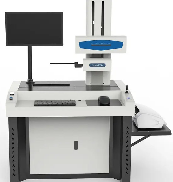
Wafers are measured for thickness, diameter, and flatness using precision instruments. Ensuring consistent dimensions is crucial, as variations can affect the wafer's performance in semiconductor manufacturing. These measurements are typically automated to ensure accuracy and repeatability.
The wafer's surface is analyzed using specialized tools like profilometers or interferometers to measure flatness and roughness. High surface flatness and minimal roughness are essential for the wafer's ability to support intricate circuit patterns in semiconductor devices.
The density of defects, such as dislocations or vacancies within the silicon crystal, is measured using techniques like X-ray topography or etching followed by microscopic inspection. Lower defect densities are preferred, as they lead to better device performance and reliability.
Automated systems measure the wafer's thickness and bow (deformation). Ensuring that wafers are within tight tolerances is crucial for compatibility with semiconductor manufacturing equipment. Excessive bowing can lead to handling issues and defects in the final product.
Wafer mapping is the systematic testing of several spots on the surface of each wafer. This comprehensive method guarantees that variations in attributes are identified and corrected, hence contributing to overall consistency.
Carrier lifetime, or the time it takes for charge carriers (electrons and holes) to recombine in the silicon, is a critical parameter for semiconductor performance. Testing for carrier lifetime helps identify defects within the crystal structure that could impact the wafer's effectiveness in electronic devices.
Electrical properties, including conductivity and breakdown voltage, are tested using various probing methods. These tests confirm that the wafer will perform correctly in electronic circuits, ensuring that it meets the stringent requirements of the semiconductor industry.

Silicon wafers are predominantly produced with a single-crystal structure, offering unmatched uniformity in electrical properties across the entire wafer. This crystallographic precision is essential for creating high-performance semiconductor devices, ensuring consistent behavior of integrated circuits.

The surface of silicon wafers can be polished to an ultra-smooth finish, with minimal surface defects and irregularities. This high-quality surface is crucial for photolithography, where even the slightest imperfection can affect the accuracy of circuit patterns.

Silicon allows for precise doping, which involves the intentional introduction of impurities to control its electrical properties. This control is critical in creating various types of semiconductor devices, including n-type and p-type regions within a single wafer, enabling the construction of complex circuits.

Silicon wafers offer a broad range of electrical resistivities, from highly conductive to highly resistive, making them suitable for different types of semiconductor devices. This flexibility allows manufacturers to tailor silicon wafers to specific applications, from power devices to high-speed processors.

Silicon's thermal conductivity is adequate for most semiconductor applications, allowing it to efficiently dissipate heat generated during device operation. This property is particularly important in high-density circuits where heat management is critical to prevent device failure.

Silicon naturally forms a robust silicon dioxide (SiO2) layer when exposed to oxygen. This oxide layer is crucial for creating stable insulating layers, especially in MOSFETs and other transistor technologies, providing excellent insulation and reliability.


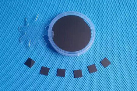
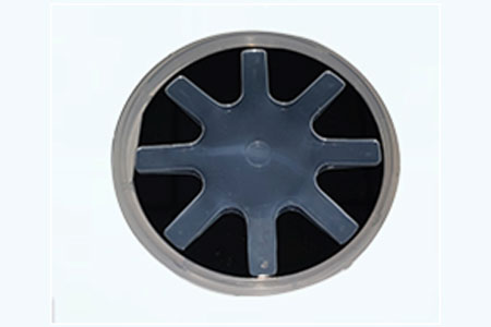
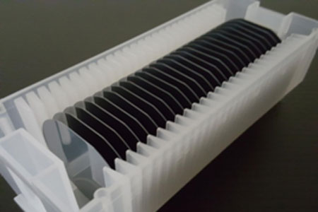
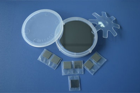
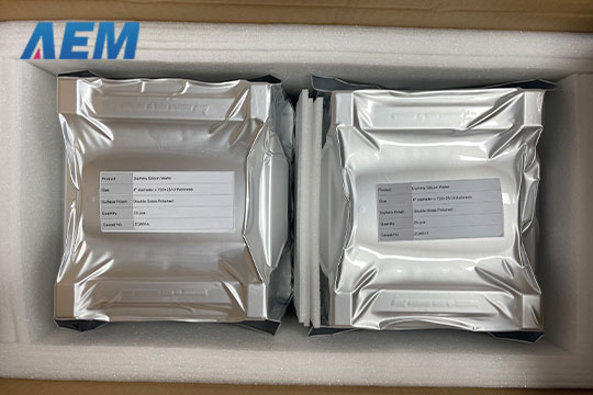
Packaged with class 100 clean bag or wafer container in a class 1000 clean room.
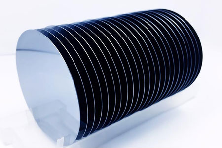
A silicon wafer is a thin slice of crystal semiconductor, such as a material made up from silicon crystal, which is circular in shape. Silicon wafers are made up of pure and single crystalline material. They are used in the manufacture of semiconductor devices, integrated circuits and other small devices.
The quality of a silicon wafer is determined by several factors, including crystal orientation, surface flatness, resistivity, purity, and the absence of defects. High-quality wafers have a smooth, polished surface with minimal impurities, making them suitable for advanced semiconductor manufacturing.
Resistivity is a key parameter in silicon wafers that indicates the wafer's ability to conduct electricity. It is crucial in determining the wafer's suitability for specific semiconductor applications, as different devices require wafers with varying resistivity levels.
Yes, silicon wafers can be customized based on specific needs, including diameter, thickness, resistivity, and crystal orientation. We offer custom wafers to meet the unique requirements of different semiconductor applications.
Monocrystalline silicon wafers consist of a single continuous crystal structure, offering higher efficiency and better electrical properties. Polycrystalline silicon wafers are made of multiple smaller crystals, which makes them less efficient but more cost-effective.
The slicing process can impact wafer quality by introducing surface damage and stress. Techniques like diamond wire saw slicing can reduce damage compared to traditional circular saws. Subsequent grinding and polishing steps are essential to correct surface imperfections and achieve the desired quality.
Higher purity silicon wafers exhibit better electrical performance and fewer defects, which is critical for high-performance semiconductor devices. Impurities can act as electrical traps or disrupt the crystal lattice, affecting the wafer's ability to function effectively in electronic applications.
Silicon wafer surfaces can be classified into different types based on their orientation and treatment. Common surface types include polished, etched, and rough surfaces. Each type is suited for different applications, such as polished surfaces for high-precision electronics and rough surfaces for certain sensors.
Yes, silicon wafers can be recycled. Reclaimed silicon from used wafers can be purified and reused to manufacture new wafers. Recycling helps reduce waste and environmental impact, making it a sustainable practice in the semiconductor industry.
Please be advised that customised specification silicon wafers require approximately 3-4 weeks for shipping. If the order is for a regular specification and we have stock, it can be shipped in 1-2 weeks. Please also understand that if transportation volume accumulates during holidays, the delivery time may be slower.
| Superconducting Substrates | |
| Magnetic Ferroelectricity Substrates | |
| Semiconductor Wafers | |
| GaN Thin Film Substrates | |
| Halide Substrates | |
| Ceramic Substrates | |
| Metal Substrates |