Sputtering Targets
Evaporation Materials
Evaporation Sources
High Purity Materials
Thin Film Substrates
Crytstal Materials


 +86-731-89578196
 [email protected]
Sputtering Targets

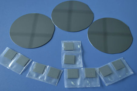
At AEM, we specialize in delivering premium GaAs wafers with exceptional precision and quality. Our advanced manufacturing techniques ensure consistent performance, positioning us as leaders in gallium arsenide technology. We are committed to innovation, continually refining our processes to meet the highest industry standards.
What sets AEM apart is our focus on customization and client satisfaction. We work closely with customers to tailor GaAs wafers to specific requirements, ensuring reliable and consistent results. Backed by rigorous quality control, our wafers provide the performance you can trust.
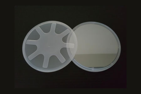
| Size | 25mmx25mm, 10mmx10mm, 10mmx5mm, 5mmx5mm,2'' Dia, 3'' Dia, 4'' Dia, 6" Dia (customized sizes are available) | ||
|---|---|---|---|
| Thickness | 350um, 650um (Tolerance: ±25um) | ||
| Polished | SSP or DSP | ||
| Orientation | <100>,<110>, <111> | ||
| Redirection Precision | ±0.5° | ||
| TTV | <10 um | ||
| Bow | <20 um | ||
| Warp | <20 um | ||
| Surface Roughness (Ra:) | <5Å | ||
| Material | GaAs |
|---|---|
| Growth Method | VGF, VB |
| Lattice (A) | a=5.653 |
| Structure | M3 |
| Melting Point | 1238℃ |
| Density(g/cm3) | 5.31 g/cm3 |
| Doped Material | Si-doped / Zn-doped/ Undoped |
| Type | N-type/P-type/ Semi-insulating |
| Carrier Concentration (cm-3) | 5 x 10¹⁷ |
| EPD (Average) | <5 x 10⁵/cm2 |
Our advanced manufacturing techniques ensure every GaAs wafer meets the highest standards of accuracy and quality.
We tailor each wafer to meet your specific needs, providing flexible solutions for diverse requirements.
Rigorous quality control ensures that each wafer delivers reliable and consistent performance across all production batches.
AEM stays at the cutting edge of gallium arsenide technology, constantly refining our processes to offer the most advanced solutions.
Our efficient production processes allow for timely delivery without compromising on quality.
Gallium arsenide single crystals are grown using methods like Liquid Phase Epitaxy (LPE) or Metal Organic Vapor Phase Epitaxy (MOVPE). Afterward, surface damage is removed, and the crystal is cut into thick slices.
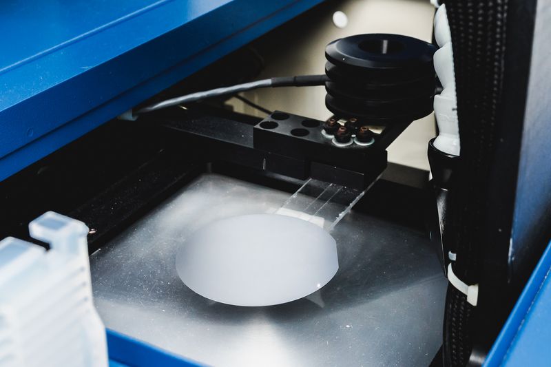
Thick slices are further cut into wafer-sized circular pieces using precise slicing equipment to control dimensions.
Wafers undergo CMP to create a smooth, flat surface through stages of coarse, medium, and fine polishing.
A photomask defines patterns on the wafer, followed by exposure, development, and post-processing.
Either dry or wet etching is used to remove materials from selective areas, allowing for chip processing.
The wafer surface is coated with metals like aluminum or copper to create conductive paths, ensuring good contact with components.
The finished wafers are tested for electrical performance through DC, RF, and contact point evaluations to ensure they meet design specifications.
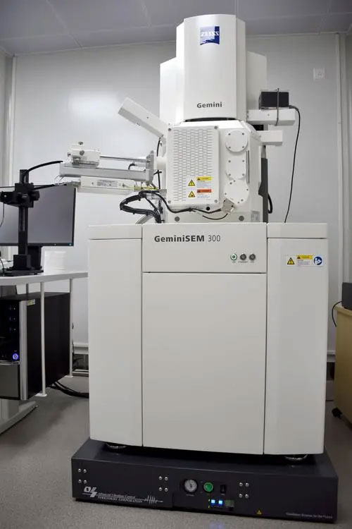
Advanced microscopes are used to check for surface imperfections like scratches, pits, or cracks. Scanning electron microscopy (SEM) may also be used for more detailed surface analysis.
The wafer's thickness, diameter, and flatness are carefully measured using precise tools like micrometers and interferometers. Flatness control is particularly important to ensure uniformity for device fabrication.
Atomic force microscopy (AFM) or profilometers measure surface roughness at the nanoscale level. A smooth surface is essential for subsequent photolithography steps.
X-ray diffraction (XRD) or Laue back reflection techniques are employed to analyze the crystal structure, orientation, and lattice quality of the GaAs wafer. This ensures that the crystal is free from defects such as dislocations or twinning, which can impact device performance.
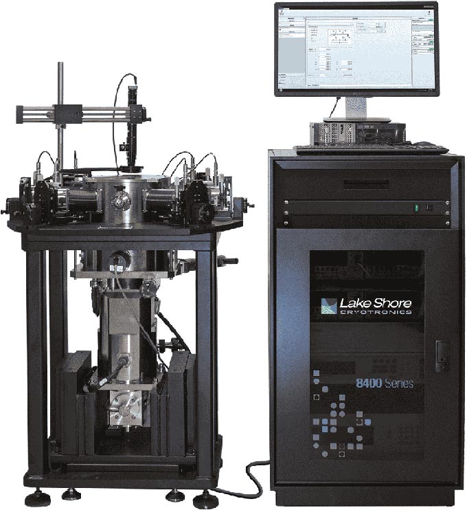
GaAs wafers are tested for critical semiconductor properties like resistivity, carrier mobility, and carrier concentration using methods such as Hall Effect measurements or four-point probe testing. These tests ensure the wafers meet required electrical specifications.
Defect density is checked using etch pit density (EPD) or cathodoluminescence to identify crystal imperfections, such as dislocations or inclusions.
Automated tools measure the uniformity of the wafer’s thickness and resistivity across the entire surface to ensure consistency. Non-uniform wafers can lead to performance issues during device fabrication.
Wafers are analyzed for chemical contamination using methods like secondary ion mass spectrometry (SIMS) or total reflection X-ray fluorescence (TXRF). Any contamination, especially from metals, can degrade wafer performance.
GaAs allows electrons to move faster compared to silicon, enabling quicker data transmission. This makes GaAs ideal for high-speed devices like microwave and millimeter-wave applications.

GaAs can efficiently emit light, unlike silicon, which has an indirect bandgap. This feature is crucial for optoelectronic devices like LEDs, laser diodes, and solar cells.

GaAs maintains high performance under elevated temperatures, offering greater thermal stability, ideal for aerospace and defense applications.

GaAs minimizes signal distortion and interference, making it ideal for applications in RF and microwave frequencies, such as satellite communications.

The high-speed signal processing capabilities of GaAs wafers allow them to support fast switching speeds, essential in radar, telecommunications, and computing.

GaAs wafers are versatile, being used in both optoelectronic and electronic applications, from communication devices to photonic circuits.

GaAs wafers are lighter than other materials used in electronics, making them highly desirable in industries like aerospace, where weight reduction is critical for performance and efficiency.
GaAs-based transistors offer higher speeds than silicon due to superior electron mobility, making them ideal for high-performance computing and processors where speed is critical.
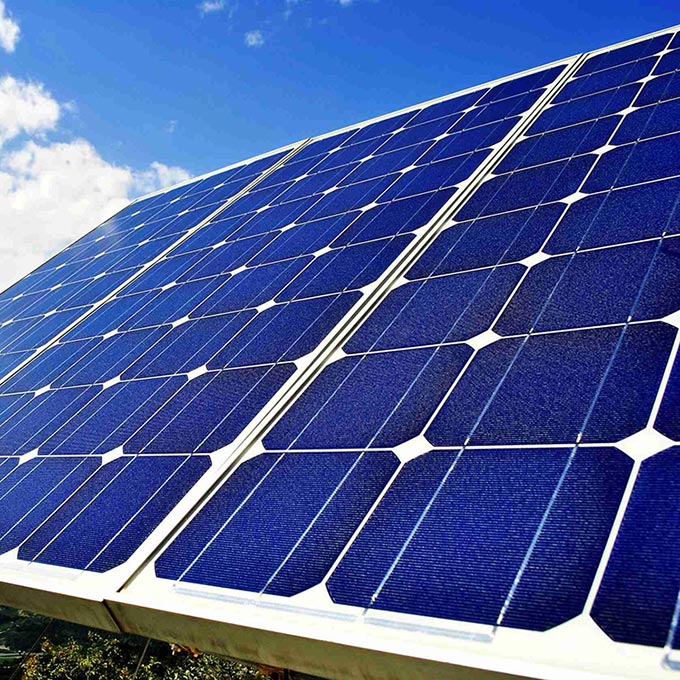
GaAs solar cells are highly efficient, especially in space applications, where they can convert sunlight into electricity even under low-light or extreme conditions, outperforming silicon-based cells.
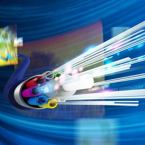
GaAs is crucial in fiber-optic communication systems, supporting high-speed data transmission over long distances with minimal signal degradation. GaAs-based devices ensure clearer signal transmission compared to silicon.
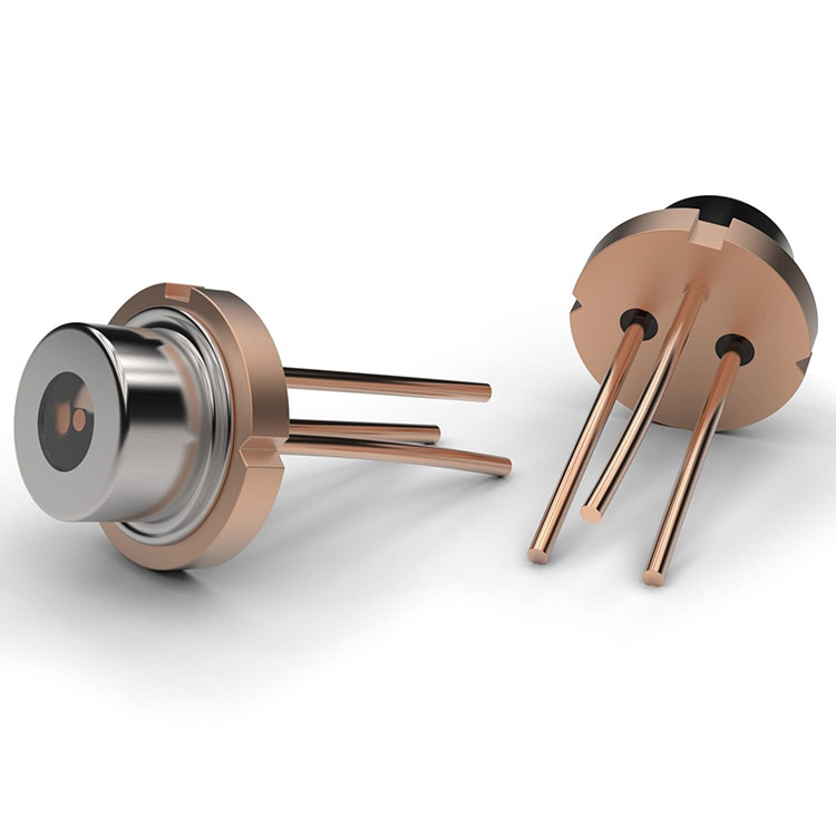
GaAs is used to manufacture laser diodes and infrared emitters for telecommunications, medical equipment, and military applications. The material’s direct bandgap allows for efficient light emission in infrared and visible ranges.
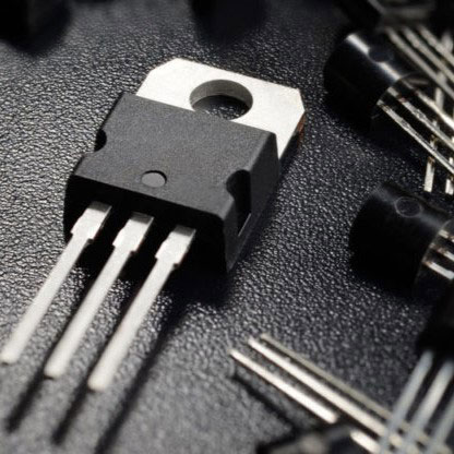
GaAs transistors, such as high electron mobility transistors (HEMTs), enable faster switching speeds and lower power consumption, making them ideal for high-frequency microprocessors.
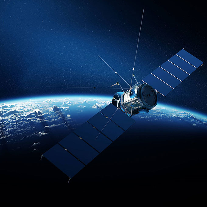
GaAs wafers are widely used in radar systems, satellite communications, missile guidance, and avionics. Their ability to perform under harsh environmental conditions, including extreme temperatures and radiation, makes them ideal for these sectors.
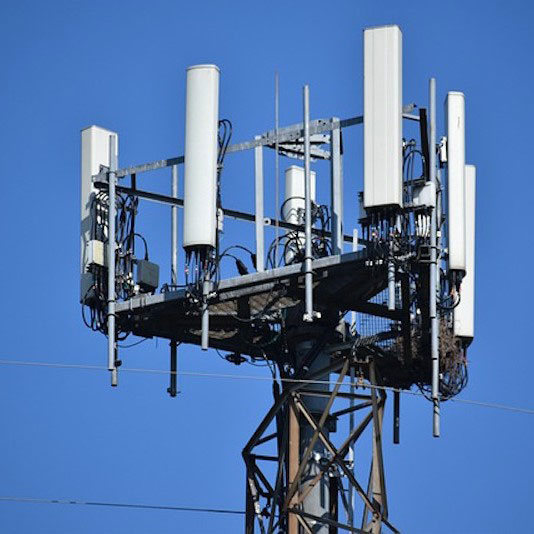
GaAs wafers are key to producing devices like microwave transistors, 5G technologies, and millimeter-wave applications. Their high electron mobility and low noise characteristics make them suitable for high-frequency operations that demand precise signal processing and speed.
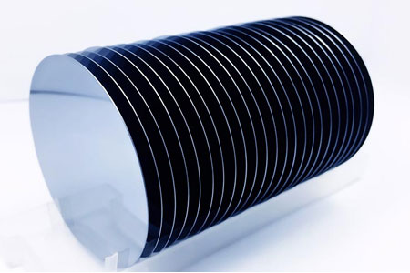
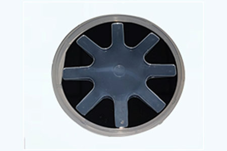
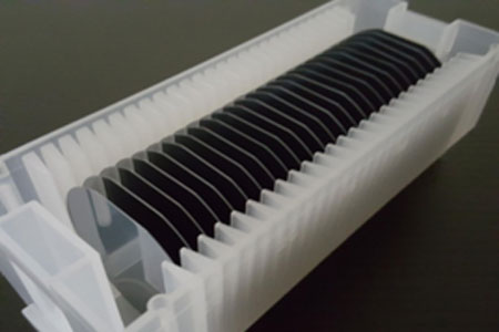
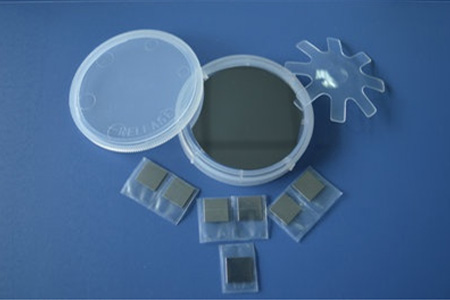
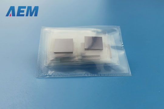
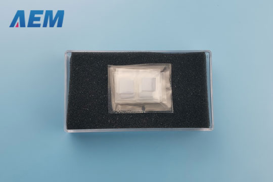
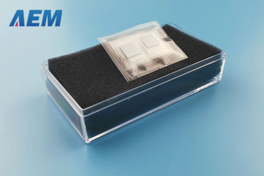
Packaged with class 100 clean bag or wafer container in a class 1000 clean room.
GaAs (Gallium Arsenide) wafers are semiconductor materials widely used in high-frequency and optoelectronic applications due to their superior electron mobility and direct bandgap properties.
Yes, GaAs wafers can be customized in terms of size, thickness, and doping levels to meet specific requirements for different applications in industries such as telecommunications, aerospace, and optoelectronics.
The primary concern is the toxic nature of arsenic in GaAs. Strict environmental and safety regulations govern the manufacturing and disposal processes to minimize health and environmental risks.
GaAs transistors produce lower noise compared to silicon, which enhances signal clarity in high-frequency applications such as telecommunications, radar, and satellite communications. This feature is particularly important for systems requiring high signal-to-noise ratios.
GaAs wafers are highly durable and can function efficiently for long periods, especially in high-temperature and high-frequency environments, making them reliable for aerospace, defense, and telecommunications.
GaAs wafers can be doped with elements such as silicon (n-type) or zinc (p-type) to modify their electrical properties, optimizing them for specific applications like high-speed transistors, LEDs, or laser diodes.
GaAs is less prone to moisture absorption compared to other semiconductors. However, prolonged exposure to harsh environmental conditions may still require protective coatings to ensure long-term stability and performance.
GaAs has relatively lower thermal conductivity compared to materials like silicon carbide, meaning heat dissipation must be carefully managed in high-power applications. Despite this, GaAs’s other advantages like high electron mobility make it ideal for RF and microwave devices.
Semi-insulating GaAs wafers are used in applications that require minimal electrical conduction, such as RF devices and microwave circuits. Semiconducting GaAs wafers, on the other hand, are doped to conduct electricity and are used in optoelectronics and transistors.
Please be advised that customised specification GaAs wafers require approximately 3-4 weeks for shipping. If the order is for a regular specification and we have stock, it can be shipped in 1-2 weeks. Please also understand that if transportation volume accumulates during holidays, the delivery time may be slower.