Sputtering Targets
Evaporation Materials
Evaporation Sources
High Purity Materials
Thin Film Substrates
Crytstal Materials


 +86-731-89578196
 [email protected]
Sputtering Targets

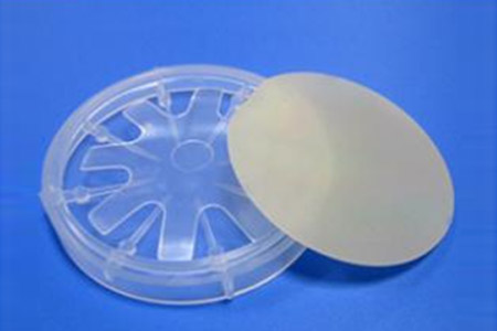
At AEM, we are dedicated to producing high-quality Gallium Nitride (GaN) wafers with a focus on exceptional craftsmanship and technological innovation. As a trusted leader in the semiconductor materials industry, we strive to deliver products that meet the highest standards of reliability and precision, ensuring our customers receive top-tier solutions for their needs.
Our Gallium Nitride wafers are known for their consistent quality and advanced manufacturing processes, setting us apart in the industry. With a strong commitment to continuous improvement, AEM is at the forefront of wafer production, helping to shape the future of technology with dependable and high-performance materials.
| Size | 10.0 mm x 10.5 mm, 14.0 x 15.0 mm, 2" Dia, 4" Dia |
|---|---|
| Thickness | 400um ±30um/450±30um |
| Polished | Front Surface: Ra < 0.2nm. Epi-ready polishedBack Surface: Fine ground |
| Orientation | C-axis(0001) ± 0.5° |
| TTV | <15 um |
| Bow | <20 um |
| Material | GaN | ||
|---|---|---|---|
| Conduction Type | N-Type | UID | Semi-Insulating |
| Resistivity(300K) | < 0.02 Ω·cm | < 0.2 Ω·cm | >1E8 Ω·cm |
| EPD (Average) | Less than 5x106 cm-2 | ||
| Useable Surface Area | > 90% | ||
| Grade | Production, Research, Dummy | ||
Every GaN wafer undergoes stringent quality checks, ensuring the highest level of consistency and reliability in each product.
Our cutting-edge production processes ensure precision in wafer thickness, uniformity, and surface finish, delivering top-tier performance.
We offer customizable options to meet specific requirements, providing flexibility in wafer specifications for diverse needs.
With years of experience in the semiconductor industry, AEM combines technical expertise with a commitment to excellence in every GaN wafer we produce.
Trusted by partners worldwide, AEM's Gallium Nitride wafers are recognized for their reliability, helping customers achieve their goals.
Gallium Nitride wafers are typically grown on substrates such as sapphire, silicon carbide (SiC), or silicon. The substrate is carefully cleaned and prepared to ensure a smooth surface for epitaxial growth. Substrate material choice is crucial, as it affects the quality and properties of the GaN layer.
GaN wafers are typically grown using techniques such as Metal-Organic Chemical Vapor Deposition (MOCVD) or Molecular Beam Epitaxy (MBE). In MOCVD, gaseous precursors like trimethylgallium (TMGa) and ammonia (NH₃) are introduced into a reactor, where they decompose and deposit a thin layer of GaN on the substrate. This process allows for the controlled growth of high-purity, defect-free GaN crystals.
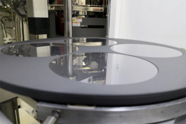
The epitaxial process continues with multiple layers of GaN being deposited on the substrate. These layers must be of precise thickness and uniformity to ensure the final wafer's quality. Controlling the temperature, gas flow, and pressure during deposition is critical to achieve the desired crystal structure.
Once the epitaxial growth is complete, the GaN wafer undergoes a chemical-mechanical polishing (CMP) process. This step smoothens the surface of the wafer and reduces surface roughness, resulting in an optically smooth and defect-free surface. The polishing process is crucial for the wafer's optical and electrical performance.
In some cases, larger GaN wafers are diced or sliced into smaller pieces. This is common in applications where smaller wafer sizes are required. The cutting process is done with precision tools to ensure minimal damage to the wafer.
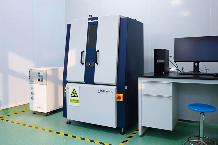
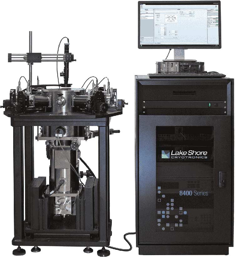
After polishing, the GaN wafers undergo rigorous inspection and testing. Parameters like surface roughness, thickness, crystal quality, and defect density are checked to ensure they meet industry standards. Testing helps verify the wafer's suitability for various electronic and optoelectronic applications.

GaN has a wide bandgap of 3.4 eV, which is significantly larger than silicon's (1.1 eV). This allows GaN-based devices to operate at higher voltages, frequencies, and temperatures, making them ideal for power electronics and high-frequency applications.

GaN wafers have excellent thermal conductivity, enabling them to dissipate heat more efficiently. This feature ensures that GaN devices can handle higher power densities and maintain stability in extreme operating environments.

The high electron mobility of GaN enables faster electron transport, leading to improved switching speeds and greater efficiency in power and RF (radio frequency) devices. This makes GaN ideal for high-speed, high-frequency applications such as 5G communication systems and radar.

GaN has a high critical electric field (breakdown voltage), allowing devices made from GaN to withstand much higher voltages without breaking down. This makes GaN wafers suitable for high-power applications, such as power converters and amplifiers, where silicon might fail.

GaN is highly resistant to radiation damage, which makes it suitable for use in aerospace, defense, and satellite applications. Its radiation hardness enables GaN wafers to maintain performance in extreme environments where other materials may degrade.

GaN wafers can operate at much higher temperatures compared to silicon, allowing devices to function effectively in harsh thermal environments. This reduces the need for complex cooling systems in power electronics, leading to more compact designs.

GaN wafers have a Mohs hardness rating close to 9, making them highly resistant to scratches and physical damage, ensuring durability and reliability in tough environments.

GaN wafers maintain excellent stability in corrosive conditions, offering strong resistance to both acidic and alkaline substances, making them suitable for chemically harsh applications.

GaN significantly enhances the performance and efficiency of automotive electronics, leading to more advanced vehicles. It also powers LiDAR systems in autonomous vehicles, enabling high-resolution 3D imaging for navigation.

GaN improves power conversion in data centers, reducing energy consumption, cooling needs, and costs, especially in machine learning and AI applications. Its high efficiency enables direct power conversion, streamlining data center operations.

GaN-based motor drives enhance precision control and efficiency in robotics and drones, improving their performance with smaller, more reliable components.

GaN-based power electronics are key in solar energy conversion, offering higher efficiency and reduced system costs for renewable energy installations.

GaN is used in consumer electronics for faster charging, higher efficiency, and compact designs. It also enables wireless power transfer in devices, from phones to household appliances.

GaN technology is transforming medical devices by enabling wireless power for implants and improving the resolution of imaging equipment, such as MRI machines and pill-sized x-ray devices.

GaN is ideal for space applications due to its natural radiation resistance, powering satellites, ion thrusters, and robotics with high efficiency in harsh environments.
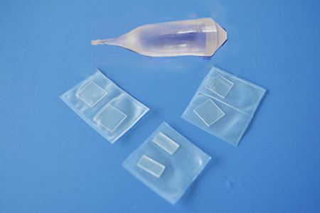
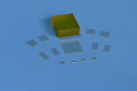
Packaged with class 100 clean bag or wafer container in a class 1000 clean room.
Gallium Nitride (GaN) wafer is a substrate made from a wide bandgap semiconductor material, GaN. It is used in the production of high-performance electronic and optoelectronic devices, including power transistors, LEDs, and radio frequency (RF) components. GaN's properties, such as high breakdown voltage, fast switching speeds, and high thermal conductivity, make it ideal for use in high-power, high-frequency, and high-temperature environments.
GaN wafers have excellent durability and longevity, particularly in harsh environments. Their high thermal and chemical resistance contributes to a longer lifespan compared to silicon wafers, making them suitable for applications where reliability and endurance are critical.
GaN technology is considered more environmentally friendly than silicon in some applications, as it enables more energy-efficient systems, reducing overall energy consumption and greenhouse gas emissions. Its use in renewable energy solutions, such as solar power conversion, further supports sustainable practices.
GaN enables more efficient power conversion in electronic devices by reducing energy losses during switching operations. Its fast switching speeds, low on-resistance, and ability to operate at high voltages contribute to higher overall energy efficiency, making it a popular choice for power electronics and renewable energy systems.
The main difference between GaN and Si wafers is their material properties. GaN is a wide bandgap semiconductor, meaning it can handle higher voltages and temperatures than silicon. GaN devices have faster switching speeds, better thermal performance, and higher power efficiency compared to silicon devices. These properties make GaN wafers more suitable for high-power, high-frequency applications, whereas silicon wafers are typically used for lower power and lower frequency devices.
Yes, GaN wafers can be integrated into existing semiconductor fabrication processes, especially those designed for compound semiconductors. However, GaN requires specialized equipment for epitaxial growth, and the fabrication process may need adjustments due to GaN's different physical and electrical properties compared to traditional materials like silicon. Many fabs are adapting to accommodate the growing demand for GaN-based devices.
The surface roughness of a GaN wafer is critical for device performance, as a smoother surface ensures better contact between layers and reduces scattering of electrons. High surface roughness can introduce defects, lower efficiency, and increase resistance in the final device. Ensuring a polished, smooth surface during wafer processing is essential to achieving optimal electrical performance.
Gallium Nitride wafers are typically grown on substrates such as silicon (Si), silicon carbide (SiC), and sapphire (Al2O3). Each substrate offers unique benefits; for example, Si is cost-effective, SiC provides excellent thermal conductivity, and sapphire is highly insulating. The choice of substrate depends on the specific requirements of the application and cost considerations.
Gallium Nitride wafers are delicate and require careful handling to prevent damage or contamination. It's important to wear gloves to avoid oils or dirt from your hands transferring to the wafer surface. They should always be handled using wafer tweezers or vacuum wands specifically designed for wafers to prevent physical damage. During storage, GaN wafers must be kept in a clean, dry, and dust-free environment, ideally in wafer carriers or cassettes. They should also be stored in antistatic packaging to prevent electrostatic discharge (ESD) that could harm the wafer's integrity.
Please be advised that customised specification gallium nitride (GaN) wafers require approximately 3-4 weeks for shipping. If the order is for a regular specification and we have stock, it can be shipped in 1-2 weeks. Please also understand that if transportation volume accumulates during holidays, the delivery time may be slower.
| Superconducting Substrates | |
| Magnetic Ferroelectricity Substrates | |
| Semiconductor Wafers | |
| GaN Thin Film Substrates | |
| Halide Substrates | |
| Ceramic Substrates | |
| Metal Substrates |