


 +86-731-89578196
 [email protected]

- Home
- Our Company
-
Products
Sputtering Targets

- Industries
- Blog
- FAQ
- Contact Us


Thin Film Deposition Methods Explained: PVD, Sputtering, Evaporation
Introduction to Thin Film Deposition
Thin film deposition is the process of adding a very thin layer of material—often only a few nanometers to a few micrometers thick—onto the surface of another material, called the substrate. This coating changes the surface’s properties while keeping the base material’s main structure and strength.
These coatings are used to improve performance in many ways. They can make surfaces conduct electricity better, allow more or less light to pass through, resist heat, reduce wear, or protect against corrosion. You’ll see thin films in semiconductors, camera lenses, solar panels, medical implants, and even aerospace components.
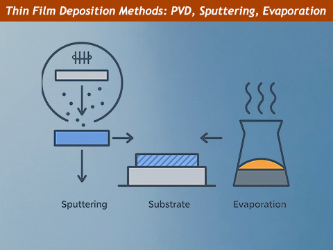
There are several ways to create these coatings. One of the most widely used is Physical Vapor Deposition (PVD), a process that turns solid material into vapor and then deposits it onto the substrate in a thin, even layer. Within PVD, two of the most common techniques are sputtering and evaporation. Each method works differently, has its own advantages, and is better suited for certain applications.
In the next sections, we’ll explain these thin film deposition methods in detail—how they work, their strengths and limitations, and how to choose the right one for your needs.
Physical Vapor Deposition (PVD) — The Core Technique
Physical Vapor Deposition (PVD) is a widely used method for creating thin films with excellent purity, uniformity, and adhesion. In PVD, the coating material starts in a solid form. Under controlled conditions, it is vaporized inside a vacuum chamber, and the vapor then condenses onto the substrate to form a thin layer.
PVD is favored in high-performance industries because:
- The vacuum environment reduces contamination, resulting in cleaner films.
- Coatings have strong adhesion to the substrate.
- It works with a wide range of materials, including metals, alloys, and certain ceramics.
There are several sub-methods under the PVD umbrella, but two stand out: sputtering and evaporation.
- Sputtering uses energetic ions to knock atoms off a target material, which then deposit onto the substrate.
- Evaporation heats the material until it turns into vapor, which travels directly to the substrate.
Both methods share the same basic principle—transforming solid material into vapor and redepositing it—but they differ in how the vapor is generated and how the coating forms. These differences affect coating quality, deposition speed, equipment cost, and the types of materials that can be used.
In the next section, we’ll take a closer look at sputtering—how it works, when it’s the best choice, and what makes it different from other deposition techniques.
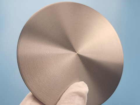
Sputtering — Precision Coatings from a Sputtering Target
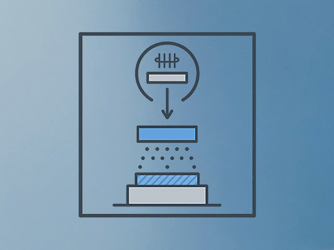
Sputtering is one of the most common and versatile thin film deposition methods used in PVD. In this process, a solid piece of material—called the sputtering target—is placed inside a vacuum chamber. The chamber is filled with a low-pressure gas, usually argon. When a high voltage is applied, the gas becomes ionized, creating a plasma.
The energetic ions from the plasma collide with the sputtering target, knocking atoms off its surface. These atoms travel through the vacuum and land on the substrate, forming a thin, uniform coating. By carefully controlling the process conditions, sputtering can produce films with precise thickness, excellent adhesion, and highly uniform coverage—even on complex shapes.
Advantages of sputtering include:
- Works with a wide variety of materials, including metals, alloys, and ceramics.
- Produces dense, high-quality films with strong adhesion.
- Allows precise control over coating thickness and composition.
- Suitable for both small-scale R&D and large-scale industrial production.
Typical applications:
- Semiconductor manufacturing
- Optical coatings for lenses and mirrors
- Transparent conductive layers in displays and solar cells
- Protective coatings for tools and medical devices
Different types of sputtering—such as DC sputtering, RF sputtering, and magnetron sputtering—offer flexibility to match the method to the material and application. Choosing the right sputtering target and sputtering method is essential for achieving the desired coating performance.
In the next section, we’ll explore evaporation—another popular PVD technique—and see how it compares to sputtering in terms of speed, cost, and film properties.
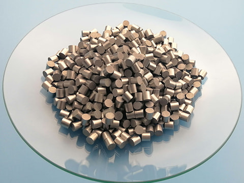
Evaporation — High-Rate Coating Using Specialized Evaporation Materials
Evaporation is another widely used thin film deposition method within the PVD family. Instead of bombarding a solid target with ions, this technique works by heating specially prepared evaporation materials until they change from a solid to a vapor. The vapor then travels through a vacuum and condenses on the substrate, forming a thin, uniform coating.
There are two main heating methods:
- Thermal evaporation – Uses a resistive heating element, such as a tungsten filament or boat, to melt and vaporize the material.
- Electron beam (e-beam) evaporation – Uses a focused high-energy electron beam to heat the material directly, making it possible to deposit high-melting-point metals.
Advantages of evaporation include:
- High deposition rates, ideal for large-area coatings.
- Simpler equipment compared to many sputtering systems.
- Cost-effective for certain metals and evaporation materials.
Limitations to consider:
- Best suited for materials that melt and vaporize cleanly.
- Coatings are typically more “line-of-sight,” which may limit coverage on complex geometries.
- Film density is often lower than sputtered films, which can reduce durability in some applications.
Common applications:
- Metallization in microelectronics
- Reflective coatings for mirrors and decorative finishes
- Optical filters and interference coatings
- Certain protective layers for wear or corrosion resistance
While evaporation can deliver faster throughput and lower costs in certain cases, sputtering is often the preferred choice when coating density, uniformity, and complex material compositions are required. In the next section, we’ll directly compare sputtering and evaporation to help you determine the best method for your project.
Sputtering vs. Evaporation — Choosing the Right Thin Film Deposition Method
Both sputtering and evaporation are proven thin film deposition methods, but their differences in process, coating properties, and cost can make one more suitable than the other depending on the project.
Below is a side-by-side comparison:
|
Feature |
Sputtering |
Evaporation |
|---|---|---|
|
Material Source |
Solid sputtering target |
Solid evaporation materials |
|
Process |
Ions knock atoms off the target surface |
Material is heated until it vaporizes |
|
Vacuum Requirement |
High vacuum |
High vacuum |
|
Deposition Rate |
Moderate |
High |
|
Film Quality |
Dense, highly uniform |
Less dense, may have columnar structure |
|
Material Compatibility |
Metals, alloys, ceramics |
Best for metals and materials with clean vaporization |
|
Substrate Coverage |
Excellent, even on complex shapes |
Mostly line-of-sight, less on complex shapes |
|
Equipment Cost |
Higher |
Generally lower |
|
Typical Applications |
Semiconductors, optics, solar coatings, precision layers |
Metallization, decorative coatings, optical filters |
Quick guidance:
- Choose sputtering when you need high-density, uniform coatings or are working with complex geometries.
- Choose evaporation when you need faster deposition rates, simpler equipment, or are working with metals that vaporize cleanly.
In the next section, we’ll share tips on how to choose the right deposition method for your material, application, and production scale.
How to Choose the Right Thin Film Deposition Method
Selecting the best thin film deposition method depends on your material, application requirements, production volume, and budget. While both sputtering and evaporation can produce high-quality coatings, each has advantages that make it more suitable in certain situations.
Key factors to consider:
- Material Type –
- For complex alloys or ceramics, sputtering targets often provide better control and consistent film quality.
- For metals that melt and vaporize cleanly, evaporation materials may offer a faster and more cost-effective solution.
- Coating Requirements –
- If you need dense, highly uniform coatings with precise composition, sputtering is usually the better choice.
- If deposition speed and large-area coverage are priorities, evaporation may be more efficient.
- Substrate Shape –
- Sputtering offers better coverage on 3D or complex geometries.
- Evaporation works best on flat or simple shapes where line-of-sight deposition is possible.
- Production Scale –
- Sputtering systems are ideal for high-precision R&D and demanding production environments.
- Evaporation systems can be more economical for high-throughput, lower-complexity coatings.
- Budget and Equipment –
- Sputtering equipment typically costs more to purchase and operate.
- Evaporation systems are generally simpler and less expensive to run.
Expert Tip: The right method is not just about the process—it’s also about using the right materials. Partnering with a reliable supplier for high-purity sputtering targets and quality evaporation materials ensures consistent results and optimal coating performance.
Final Thoughts
Thin film deposition plays a key role in many modern products, from the chips in electronics to the coatings on solar panels and camera lenses. Two of the most widely used methods are sputtering and evaporation. Each has its own strengths—sputtering offers precise, uniform coatings, while evaporation can be faster and more cost-effective for certain materials.
The right choice depends on your needs: the type of material, the coating quality you want, the shape of your parts, and your production scale. In many cases, the quality of the sputtering targets or evaporation materials you use can make just as much difference as the process itself.
At AEM Deposition, we provide high-purity thin film materials in custom sizes and purities, designed to meet the demands of both research projects and large-scale manufacturing. We can help you choose the right materials and method to get the best performance for your application.
Contact us today to get expert advice or request a quote for sputtering targets or evaporation materials for your next project.