


 +86-731-89578196
 [email protected]

- Home
- Our Company
-
Products
Sputtering Targets

- Industries
- Blog
- FAQ
- Contact Us


Silicon Wafer Manufacturing: Key Processes & Technologies
Silicon wafers are crucial for devices like smartphones, computers, and solar panels. However, the manufacturing process is complex and often misunderstood. This article simplifies the key steps and technologies involved in making silicon wafers.
We start with how pure silicon ingots are made and then cut and polished into thin wafers. We explain important methods like the Czochralski and Float Zone techniques and how they affect wafer quality.
We'll also look at new advancements in wafer manufacturing, such as using advanced growth techniques and integrating machine learning and automation. These innovations improve wafer performance and support the development of better electronic devices.
Join us to uncover the essential processes and technologies behind silicon wafer manufacturing and how they shape our digital world.
Importance of Silicon Wafers in the Semiconductor Industry
Silicon wafers are essential in the semiconductor industry as the base for integrated circuits (ICs) and other electronic components. These thin silicon slices offer a flat, smooth surface for creating electronic circuits. The purity and quality of silicon wafers directly impact the performance and reliability of the devices they are used in.
The demand for silicon wafers has surged due to the rapid growth of the electronics industry. As devices become smaller, faster, and more powerful, manufacturers need more advanced silicon wafers. Understanding the key processes in silicon wafer manufacturing is vital for developing cutting-edge electronic devices.
Key Processes in Silicon Wafer Manufacturing
Crystal Growth and Slicing: From Silicon Ingots to Wafers
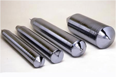
The first step in making silicon wafers is producing high-purity silicon ingots. This is done using two main techniques: the Czochralski method and the Float Zone method.
In the Czochralski method, high-purity polycrystalline silicon is melted in a crucible. A single crystal seed is slowly pulled from the molten silicon, rotating as it solidifies into a cylindrical ingot.
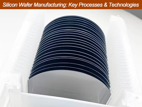
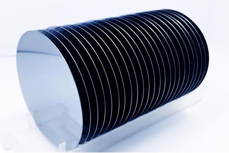
Once the ingot is formed, it is sliced into thin wafers using precision sawing. These wafers are circular discs, typically 200mm, 300mm, or larger in diameter. The thickness of the wafers varies from 200 to 1000 micrometers, depending on their intended use.
Wafer Polishing and Cleaning: Achieving the Desired Surface Quality
After slicing, the wafers are polished to create a smooth, flat surface. This step is crucial because imperfections can affect the performance of electronic circuits built on the wafers. Mechanical polishing is typically used, involving the wafers being held against a rotating polishing pad with abrasive particles and chemicals.
After polishing, the wafers are thoroughly cleaned to remove any contaminants or particles from the manufacturing process. This cleaning step ensures the wafers are free from impurities that could harm the performance and reliability of electronic devices.
Doping and Diffusion: Controlling Electrical Properties
To make electronic components like transistors and diodes, wafers go through doping. This means adding impurity atoms like boron and phosphorus into the silicon crystal to change how it conducts electricity.
After doping, the wafers are heated in a process called diffusion. This spreads the impurity atoms evenly through the silicon, creating a controlled concentration. Diffusion is vital for controlling how the wafers conduct electricity and ensuring the electronic components work correctly.
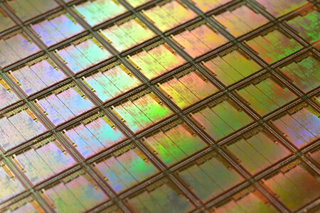
Photolithography: Creating Circuit Patterns
In this step, photolithography makes the intricate patterns needed for the electronic circuitry on the wafers. First, a light-sensitive material called photoresist is applied to the wafer's surface. Then, the wafer is exposed to ultraviolet light through a photomask, which has the desired circuit pattern.
The exposed areas of the photoresist become either soluble or insoluble, depending on the type of resist used. After that, the wafer is developed, removing the soluble parts of the photoresist. The remaining photoresist acts as a protective layer, allowing selective etching or deposition of materials to create the circuit features.
Etching and Deposition: Building Circuit Features
Etching and deposition are important steps in making silicon wafers and creating circuit features.
Etching selectively removes layers of silicon or other materials from the wafer's surface using chemical or plasma etchants. This helps create trenches, vias, and other structures needed for the circuitry.
Deposition adds thin layers of materials onto the wafer's surface. This can be done in various ways like chemical vapor deposition (CVD) or physical vapor deposition (PVD). Deposition helps create insulating layers, conductive interconnects, and other essential parts of electronic circuits.
Metrology and Inspection: Ensuring Quality and Accuracy
Throughout the silicon wafer manufacturing process, metrology and inspection are crucial for ensuring quality and accuracy.
Metrology involves measuring and characterizing various parameters like thickness, flatness, and surface roughness. Techniques such as optical microscopy, scanning electron microscopy (SEM), and atomic force microscopy (AFM) are used to analyze the wafer properties.
Inspection is about spotting defects or anomalies on the wafers. Automated inspection systems with advanced imaging and pattern recognition are used to scan for abnormalities. This helps manufacturers find and fix any issues before using the wafers in electronic device production.
Cutting-Edge Advances in Silicon Wafer Technology
As we keep demanding more advanced electronics, manufacturers keep finding new ways to improve silicon wafer production. Some cool new technologies have come up lately that are changing the game and making even better electronic devices possible.
One big deal is how they're growing really thin layers of crystal material on silicon wafers. This process, called epitaxy, lets them control how these layers turn out, making them super efficient or using less power. This means the electronic devices they make can work even better.
Another thing that's making a difference is using machine learning and automation technologies. Machine learning algorithms can go through loads of data collected during manufacturing. This helps manufacturers find better ways to do things and make their operations smoother.
Automation technologies, like robots and special systems for handling wafers, are also helping out. They make things run smoother and cut down on mistakes made by people. All of this means they can make more wafers and spend less money doing it.
Conclusion: The Future of Silicon Wafer Manufacturing
In this article, we've uncovered the secrets of silicon wafer manufacturing, explaining the important steps and high-tech methods that make it all work. From growing crystals to slicing wafers and cleaning them up, every part of the process is crucial for making top-notch wafers.
Plus, new techniques like advanced crystal growth and smart technology are opening up exciting possibilities for making even better electronic gadgets.
Our company AEM is a leading wafer and substrate manufacturer in China. Contact our sales team anytime for your product needs.