+86-731-89578196
 [email protected]

- Home
- Our Company
-
Products
Sputtering Targets

- Industries
- Blog
- FAQ
- Contact Us


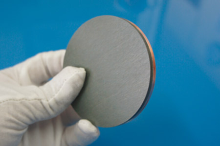
Innovations of Sputtering Targets
New photovoltaic applications, thermoelectric, storage, and semiconductor markets spur innovation in ceramic and semiconductor sputtering targets. Magnetron sputtering is initially developed using metal or alloy targets with materials having high electrical conductivity (e.g., Al, Ag, Au, Cu, Ti, Mo.). To achieve acceptable deposition rates, the target material needed to be electrically and thermally conductive. Ceramic sputtering targets are developed for transparent conductive oxides (TCOs) and are usually consisted of films made from compositions of ZnO: Al2O3 (2% wt) or In2O3:SnO2 (10% wt). However, as the name implies, the materials are fairly conductive and are suited for DC magnetron sputtering.
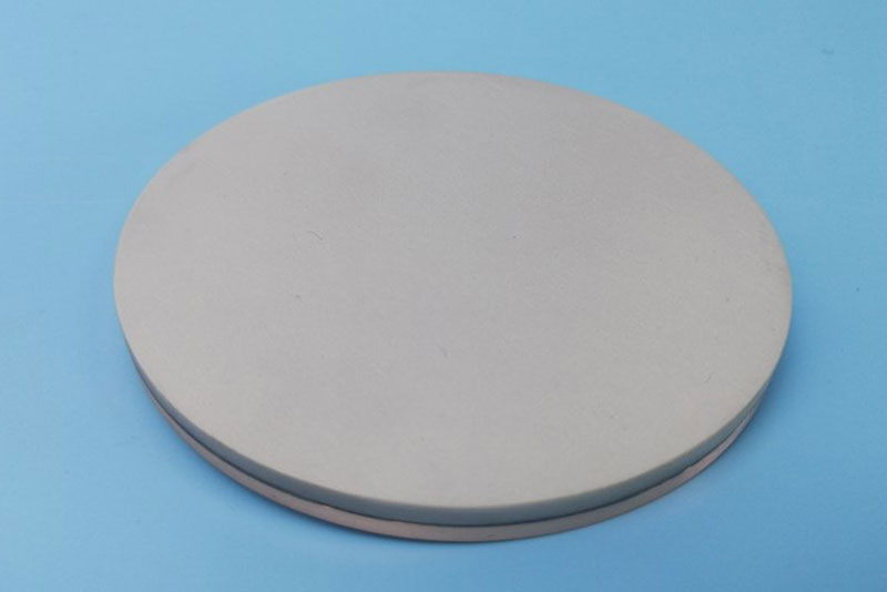
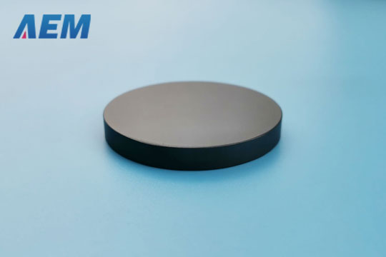
Pulsed-DC and RF magnetron sputtering allows for the deposition of materials with poor electrical conductivity. Semiconductor materials with better electrical conductivity can be sputtered with pulsed-DC power supplies, while insulating materials (mainly ceramics) require RF sputtering. The deposition rates for RF sputtering are generally much lower than with pulsed-DC. Also, pulsed-DC sputtering has a lower deposition rate than DC sputtering. New photovoltaic applications, thermoelectric, storage, and semiconductor markets are spurring innovation in ceramic and semiconductor sputtering targets.DC sputtering with metallic targets has fewer process problems since the metals are ductile, and the materials feature high conductivity. Conversely, semiconductors and ceramic sputtering targets are more prone to process difficulties due to the materials' brittle nature and poor electrical and thermal conductivities. In order to achieve consistent sputtering over the life of the target, it is essential to have a well-sintered target material with high-density. Voids and cracks in the material can propagate and lead to sputtering problems such as arcing, target cracking, and particle generation.