


 +86-731-89578196
 [email protected]


- Home
- Our Company
-
Products
Sputtering Targets
- Industries
- Blog
- FAQ
- Contact Us
Silicon Carbide (SiC): Properties, Applications, and Material Forms
views, Updated: 2026-11-10
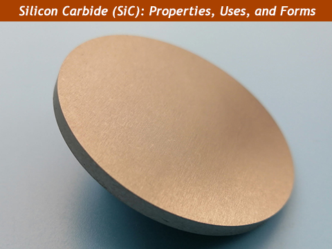
Silicon carbide (SiC) is a compound of silicon and carbon. It is hard, conducts heat well, and can serve as a wide-bandgap semiconductor. Its hardness makes it useful in abrasives and wear-resistant parts, while its electrical properties make it suitable for high-voltage power devices.
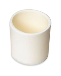
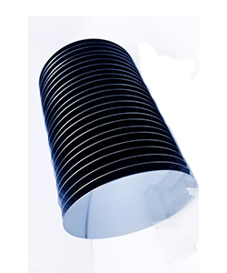
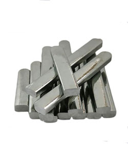
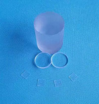
The right form of SiC depends on the job. A SiC substrate provides a surface for growing a semiconductor layer. A SiC sputtering target supplies material for depositing a thin film. A SiC crucible holds metal during melting, while a SiC single crystal can serve as a sample for materials research.
What Is Silicon Carbide?
Silicon carbide contains equal numbers of silicon and carbon atoms. In crystalline SiC, these atoms form layers that can stack in different patterns. Each stacking pattern is called a polytype. The chemical formula stays the same, but the crystal structure can change how the material behaves.· 3C-SiC has a cubic crystal structure. It is studied for thin-film applications, including microsensors.
· 4H-SiC has a hexagonal crystal structure. It is widely used in wafers for high-voltage power devices.
· 6H-SiC also has a hexagonal structure, with a different stacking pattern from 4H-SiC.
When specifying a SiC substrate, check which polytype your process requires. Two wafers can have the same diameter and thickness while having different electrical properties.
What Are the Key Properties of Silicon Carbide?
Hardness and Wear Resistance
Silicon carbide is very hard and resists scratching and abrasion. In a grinding wheel, hard SiC particles remove material from a workpiece. In a wear-resistant component, that same hardness helps the surface hold up against repeated contact with abrasive particles.Thermal Conductivity
Silicon carbide conducts heat well. In a power device, a SiC substrate helps move heat away from the active area toward the package. Thermal conductivity varies by grade and material form, so use the value for the specific material when comparing options.Wide Bandgap and High Breakdown Field
A wide bandgap means that more energy is needed to free electrons so they can carry current. This helps limit leakage current as the device heats up. A high breakdown field means the material can withstand a stronger electric field before electrical breakdown occurs. Together, these properties help explain why 4H-SiC is widely used in high-voltage power devices.
How Is Silicon Carbide Made?
Silicon carbide is made in different ways depending on the final product. Abrasive grains are crushed and sorted by size. Wafers are sliced from a grown crystal, while sputtering targets can be formed from SiC powder using heat and pressure.SiC Grains and Powders
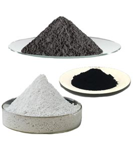
In the Acheson process, silica and a carbon source such as petroleum coke react at high temperature in an electric furnace. After cooling, the resulting silicon carbide is crushed, milled, and sorted by particle size. Coarser grains can be used in grinding wheels, while finer grades are used for surface finishing.SiC Single Crystals and Wafers
Most commercial SiC wafer production starts with physical vapor transport (PVT). SiC powder is heated in a graphite crucible to a temperature that can be around 2,300 °C. The powder sublimates, and the vapor travels to a cooler seed crystal. SiC grows on the seed over time, forming a large single crystal called a boule.The boule is cut at a controlled angle to give the wafers the required crystal orientation. The wafers are then ground and polished to achieve the specified thickness and surface finish.
SiC Sputtering Targets
AEM Deposition uses hot-press sintering to consolidate SiC powder into a dense target blank. The blank is finished to the required dimensions. When the assembly calls for an elastomer bond, the finished target is attached to a backing plate using a flexible bonding layer.Before shipment, the target is cleaned for use in a vacuum system. Final packaging helps keep contaminants off the cleaned surface and protects the target during transport.
What Is Silicon Carbide Used For?
Power Electronics and Semiconductor Manufacturing
Silicon carbide is used to make power devices such as MOSFETs and diodes. These devices control the flow of electricity in EV inverters, industrial motor drives, and power supplies. In an electric vehicle, for example, the inverter uses power devices to convert battery power into the alternating current that drives the motor.SiC wafers can also serve as a base for growing gallium nitride (GaN). In this case, the GaN layer is used to make the active device, while the SiC substrate supports the layer and helps carry heat away. One example is GaN-on-SiC used in radio-frequency amplifiers.
Thin Films and Coatings
A thin SiC layer can add wear resistance to a surface or form part of a microsensor. The deposition method depends on the film the application needs. In sputtering, a SiC target can supply the material that forms the film. In chemical vapor deposition (CVD), gases react at or near the substrate surface to form the SiC layer.Engineering Ceramics, Abrasives, and Metal Melting
In grinding wheels and abrasive papers, hard SiC grains cut or finish a surface. In ceramic components, SiC helps parts withstand repeated wear. SiC-based crucibles serve a different purpose. Foundries use them to hold and melt nonferrous metals such as aluminum and copper alloys.
Silicon Carbide Forms Available from AEM Deposition
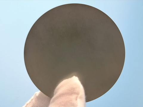
AEM Deposition offers silicon carbide in three forms for semiconductor fabrication, thin-film deposition, and materials research. The right choice depends on whether you need a wafer to build on, a target to deposit from, or a crystal sample to study.
Silicon Carbide Substrates
Our SiC substrates are available as wafers for semiconductor fabrication and thin-film growth, including gallium nitride (GaN) growth. When requesting a quote, specify the wafer diameter, thickness, crystal orientation, and whether you need one or both sides polished. View our silicon carbide substrates.Silicon Carbide Sputtering Targets
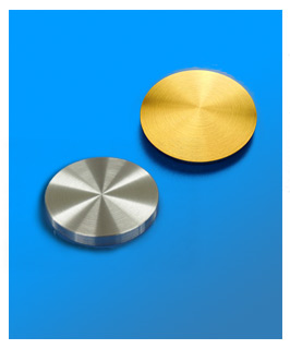
Our planar SiC sputtering targets supply material for depositing silicon carbide thin films. We list a minimum purity of 99.5% and offer target bonding. To help us match the target to your system, share the target dimensions and any backing plate or bonding requirements. View our silicon carbide sputtering targets.Silicon Carbide Single Crystals
We offer SiC single-crystal samples for materials research. If your experiment calls for a specific crystal structure or orientation, include it along with the sample dimensions and any surface preparation requirements. View our silicon carbide single crystals.
Silicon Carbide vs. Silicon: How to Choose Substrates, Targets, and Crystals
The choice between silicon carbide (SiC) and silicon (Si) depends on the job the material needs to do. For a substrate, start with the layer you plan to grow. For a sputtering target, start with the film composition. For a single crystal, start with the structure your experiment requires.SiC vs. Silicon Substrates
For GaN growth, both SiC and silicon can serve as substrates. SiC conducts heat better, which makes it useful for high-power RF devices where heat removal matters. Silicon is generally less expensive and can be a good fit for GaN power electronics when the process is designed for GaN-on-silicon. If your process already specifies one substrate, check with your growth team before switching. The substrate affects how the GaN layer is grown.SiC vs. Silicon Sputtering Targets
Choose a SiC sputtering target when your process calls for depositing a silicon carbide film from a compound target. Choose a silicon sputtering target for an elemental silicon film or for a reactive sputtering process that uses oxygen or nitrogen to form silicon oxide or silicon nitride. For a purchase inquiry, specify the film you want to deposit and the target material your process uses.SiC vs. Silicon Single Crystals
Choose a SiC single crystal when your research calls for a specific SiC polytype, such as 4H-SiC or 6H-SiC. Choose a silicon single crystal when your experiment requires elemental silicon with a defined orientation, such as Si(100) or Si(111). For a SiC sample, specify both the polytype and the surface orientation. The polytype identifies how the atomic layers stack, while the orientation identifies which crystal plane is exposed at the surface.
Conclusion
Silicon carbide has long been used in abrasives and wear-resistant parts. Today, it is also used in power electronics and thin-film coatings. The right form depends on what the material needs to do in your process.At AEM Deposition, we supply SiC substrates, sputtering targets, and single crystals for research and production.
If you're sourcing silicon carbide, contact us and send your application and specifications. Our team can help you choose a suitable option and prepare a quote.
LATEST NEWS