Sputtering Targets
Evaporation Materials
Evaporation Sources
High Purity Materials
Thin Film Substrates
Crytstal Materials


 +86-731-89578196
 [email protected]
Sputtering Targets

AEM stands out as a leader in silicon carbide wafer production, offering unmatched quality and innovation. Our expertise and cutting-edge technology enable us to deliver solutions that meet the evolving demands of high-tech industries.
What sets us apart is our dedication to customization and precision. At AEM, we focus on providing tailored solutions and exceptional service, ensuring that our wafers meet your unique needs for future-ready applications.
| Size | 10x3, 10x5, 10x10, 15x15, 20x15, 20x20, Dia15, Dia 20, Dia 1'', Dia 2'', Dia 4", Dia 6'' |
|---|---|
| Thickness | 0.35 mm |
| Crystal Orientation | <0001> |
| Polished | SSP or DSP |
| Redirection Precision | ±0.5° |
| Redirection the Edge | 2°(special in 1°) |
| Angle of Crystalline | Special size and orientation are available on demand. |
| Ra: | ≤5Å(5µm×5µm) |
| Material | SiC |
|---|---|
| Growth Method | MOCVD |
| Crystal Structure | M6 |
| Lattice (A) | a=3.08, c=15.08 |
| Direction | <0001> 3.5 º |
| Density(g/cm3) | 3.21 g/cm3 |
| Hardness | 9.2(Mohns) |
| Melting Point | 1900℃ |
| Heat Traveling @300K | 5 W/ cm.k |
| Dielectric Constants | e(11)=e(22)=9.66 e(33)=10.33 |
Our wafers are produced with the highest standards of precision and consistency to ensure top-tier performance.
We offer tailored solutions to meet your specific project requirements, providing flexibility in size, thickness, and other key parameters.
With advanced manufacturing techniques, we deliver products that align with the latest innovations in the industry.
With years of experience in the field, we have a deep understanding of silicon carbide wafer production, ensuring reliable and high-performance results.
Our strong production capabilities ensure timely delivery and consistent supply for your long-term needs.
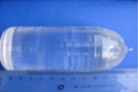
High-purity silicon powder and high-purity carbon powder are used to grow SiC single crystals through the Physical Vapor Transport(PVT) method. The raw materials are vaporized and transported to a cooler region where the SiC crystals form.
The SiC crystal is sliced into thin wafers using multi-wire dicing equipment. Each wafer is typically less than 1 mm thick to prepare it for further processing.
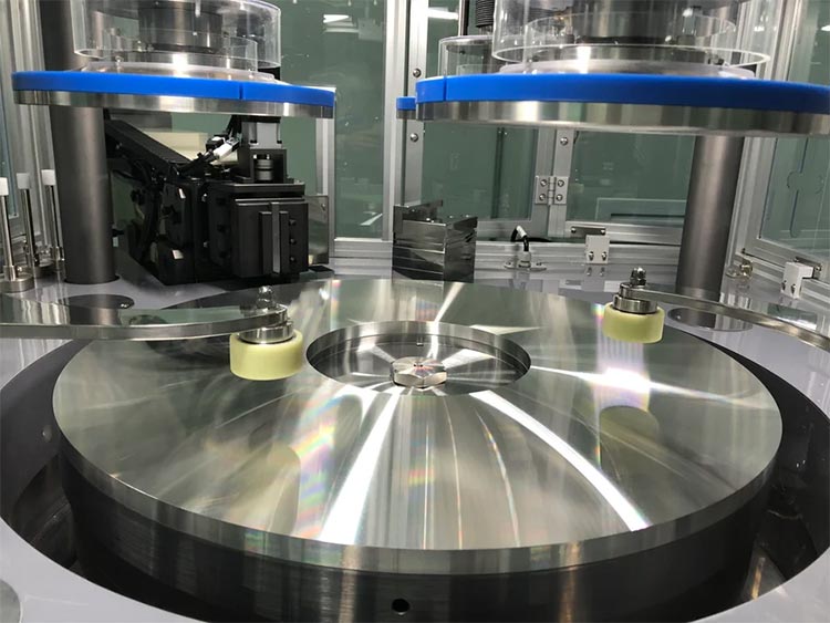
The wafers undergo grinding with diamond slurry of varying particle sizes to achieve the desired flatness and surface roughness.
The wafers are polished using mechanical and chemical-mechanical polishing techniques. This step produces a smooth, mirror-like surface, ensuring the wafers are ready for further inspection and device fabrication.
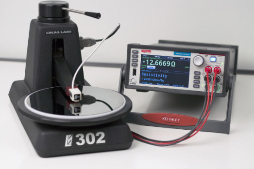
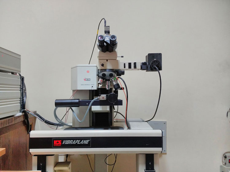
The polished wafers are examined using optical microscopes and specialized instruments to detect any defects, such as micropipe density, surface roughness, resistivity, warp, total thickness variation (TTV), and surface scratches.
SiC wafers are cleaned with specialized cleaning agents and ultrapure water to remove any surface contaminants, including polishing residues. They are then dried using ultra-high-purity nitrogen gas and a drying machine to prepare them for the next step.
Chemical Vapor Deposition (CVD) is used to grow a thin epitaxial layer of SiC on the wafer substrates. This layer enhances the performance and electrical properties of the wafers and is critical for device performance in power electronics and semiconductor applications.

SiC wafers offer a wide range of tolerance levels, allowing manufacturers to tailor the wafer characteristics to meet the specific requirements of various device fabrication processes.

High crystal quality ensures fewer defects, such as micropipes and dislocations, enhancing the reliability and longevity of devices made with SiC wafers.

SiC wafers excel in heat dissipation, allowing devices to operate efficiently at high temperatures without compromising performance, making them ideal for high-power applications.

The wide bandgap of SiC wafers provides higher breakdown voltages, which is crucial for power devices that need to withstand high electrical fields while maintaining efficiency.

SiC wafers enable devices with higher power density, supporting compact designs and efficient energy use in sectors such as electric vehicles, solar inverters, and industrial motors.

SiC wafers exhibit stable electrical properties, ensuring consistent device performance even under harsh operating conditions like high voltage and frequency.

SiC wafers have exceptionally high hardness, allowing them to withstand high pressure, friction, and other demanding conditions, making them suitable for harsh environments.

SiC wafers offer excellent electrical insulation, minimizing the risks of leakage and breakdown, which ensures the reliability and safety of electronic devices.


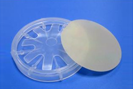
Packaged with class 100 clean bag or wafer container in a class 1000 clean room.
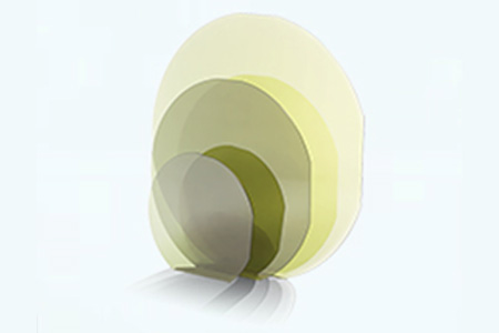
A silicon carbide (SiC) wafer is a type of semiconductor wafer made from silicon carbide, a compound of silicon and carbon. It is known for its high thermal conductivity, hardness, and electrical stability, making it ideal for power electronics, high-temperature, and high-frequency applications.
Compared to traditional silicon wafers, SiC wafers have a wider bandgap, allowing them to handle higher voltages and temperatures. SiC wafers also offer better thermal conductivity, making them ideal for high-power and high-temperature environments, while silicon wafers are more suited for low-power applications.
SiC wafers are harder and more brittle than traditional silicon, making them more difficult to process and polish. Additionally, the production of high-quality SiC wafers with minimal defects requires advanced techniques like chemical vapor deposition (CVD) and physical vapor transport (PVT).
SiC wafers contribute to energy efficiency in various applications, which helps reduce overall energy consumption and carbon emissions. Their use in renewable energy systems and electric vehicles also supports the transition to greener technologies.
N-type SiC wafers have an excess of electrons (negative charge carriers), while p-type SiC wafers have an excess of holes (positive charge carriers). The doping process determines whether the wafer is n-type or p-type, and these types are used in different semiconductor devices, such as diodes and transistors.
SiC wafers are used to fabricate a range of devices, including diodes, MOSFETs, IGBTs, and power transistors. These devices are commonly used in power electronics for applications like electric vehicles, renewable energy systems, industrial motors, and high-frequency RF systems.
Larger-diameter SiC wafers, such as 6-inch or 8-inch wafers, provide economies of scale by allowing more devices to be fabricated on a single wafer. This reduces the cost per device and increases production efficiency, especially for high-volume semiconductor manufacturing.
SiC wafers undergo rigorous cleaning processes to remove surface contaminants. After polishing, wafers are typically cleaned using specialized cleaning agents and ultra-pure water to eliminate residues like polishing compounds. They are then dried using high-purity nitrogen gas to ensure a contamination-free surface for subsequent processing.
Doping involves adding impurities to SiC wafers to modify their electrical properties. N-type doping introduces elements like nitrogen to create more free electrons, while p-type doping uses elements like aluminum to create more holes. Doping enables precise control over the wafer’s conductivity, which is crucial for fabricating semiconductor devices.
Please be advised that customised specification silicon carbide wafers require approximately 3-4 weeks for shipping. If the order is for a regular specification and we have stock, it can be shipped in 1-2 weeks. Please also understand that if transportation volume accumulates during holidays, the delivery time may be slower.
| Superconducting Substrates | |
| Magnetic Ferroelectricity Substrates | |
| Semiconductor Wafers | |
| GaN Thin Film Substrates | |
| Halide Substrates | |
| Ceramic Substrates | |
| Metal Substrates |