+86-731-89578196
 [email protected]

- Home
- Our Company
-
Products
Sputtering Targets

- Industries
- Blog
- FAQ
- Contact Us


Thin Film Coating Deposition
Chemical Deposition
Chemical deposition is a process by which a substrate is fully submerged in a chemical fluid, and then the material is deposited on the surface in a conformal pattern. This means every surface of the substrate is equally coated. The most common types of chemical deposition are:
1. Plating
In the plating process, a substrate is submerged in a chemical bath, often composed of water mixed with metal salts destined for deposition. The metal salts adhere to the substrate in a uniform pattern, building up a thicker film the longer the substrate is submerged. A more specialized form of plating, known as electroplating, requires the use of electricity. The substrate is connected to an anode poured by an external battery or rectifier. When the electricity is turned on, the liquid's metal particles begin adhering to the substrate surface through oxidation. Although different metals adhere at varying speeds and thicknesses, the general rule for electroplating is the higher the charge. The longer the current is connected, the thicker the deposition coating.
2. Chemical Solution Deposition (CSD)
CSD is a process very similar to plating, except that instead of metal salts in a water bath, organometallic powders in an organic solvent carry out the deposition procedure. CSD is cheaper and simpler than plating techniques, although its results are comparable.
3. Chemical Vapor Deposition (CVD) CVD does not use a liquid bath but rather involves a substrate placed in a pressurized chamber full of organometallic gas. Typical organometallic gasses include polysilicon, silicon dioxide, and silicon nitride. The gas either reacts with the substrate surface or slowly dissolves over it, depositing the thin-film evenly. A more specialized variant of CVD is plasma-enhanced CVD. Plasma is an ionized vapor and is attracted to the surface of a substrate when excited by electric currents or microwaves.
Physical Deposition
Physical deposition techniques do not include chemical reactions. They rely on mechanical or thermodynamic methods to produce thin-films instead. Generally, they require low-pressure environments for accurate and functional results.
1. Thermal evaporation
In a high vacuum, the deposition material is melted by an electric resistance heater until it covers the substrate's surface. The vacuum is required to make sure there is not an unwanted reaction between the film material atoms and gas atoms. A variant of thermal evaporation uses an electron beam evaporator to melt materials on a substrate. Because of the added precision, lower vapor pressure materials can be melted than in standard thermal evaporation.
2. Sputtering
Sputtering occurs when a noble gas plasma is shot at a substrate in atom-sized particles. The particles' impact triggers a collision cascade, which results in many of the particles passing through the substrate and adhering to the opposite side. In this manner, the entire surface of a substrate is coated.
3. Pulsed Laser Deposition
Pulsed laser deposition involves a substrate and a block of film material in an ultra-high vacuum chamber. A laser fires pulsed bursts of light at the block of material, which vaporizes and transfers to the substrate facing it. Sometimes the pulsed laser deposition occurs in an oxidated chamber so that oxygen can aid in oxide deposition.
4. Cathodic Arc Deposition (Arc-PVD)
Arc-PVD is very similar to pulsed laser deposition, except for an electric arc instead of a pulsed laser. An electric arc is an electrical charge of gas between an anode and a cathode, with the substance material serving as the cathode in Arc-PVD. As the substance material vaporizes, it condenses on the substrate and forms a thin-film.
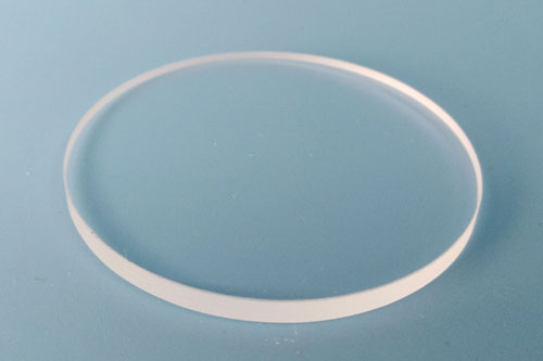
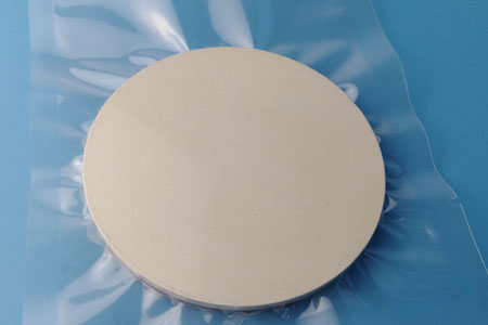
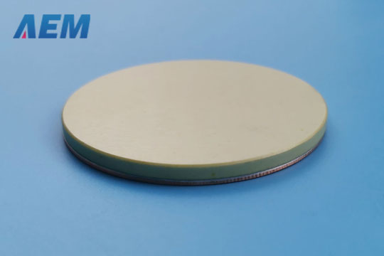
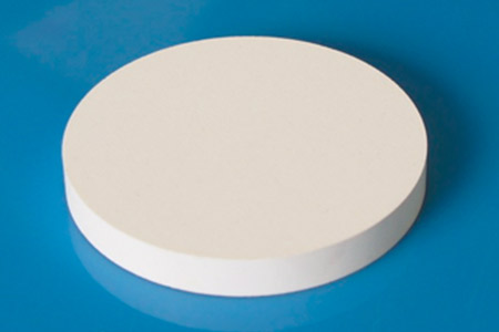
Thin Film Deposition Materials
Thin-film deposition materials are not limited to sputtering targets and evaporation materials. For more information on types of thin-film coating deposition, please pay sustained attention to AEM Deposition. By the way, AEM Deposition also is an excellent thin-film deposition materials supplier. We provide high-quality sputtering targets (target bonding services also provide), evaporation materials, and other thin-film coating deposition materials.