


 +86-731-89578196
 [email protected]


- Home
- Our Company
-
Products
Sputtering Targets
- Industries
- Blog
- FAQ
- Contact Us
What Is Sputtering? A Complete Guide to Thin Film Deposition
views, Updated: 2026-07-17
Introduction: Why Sputtering Matters in Modern Manufacturing
Sputtering is a widely used thin film deposition technology that helps create extremely thin and uniform coating layers on different materials. It is a type of physical vapor deposition (PVD) process that uses a solid material called a sputtering target as the coating source.
Today, sputtering is an important process in many advanced industries, including semiconductor manufacturing, display production, solar panels, optical coatings, and electronic devices. It allows manufacturers to add functional layers that improve electrical performance, durability, optical properties, or surface protection.
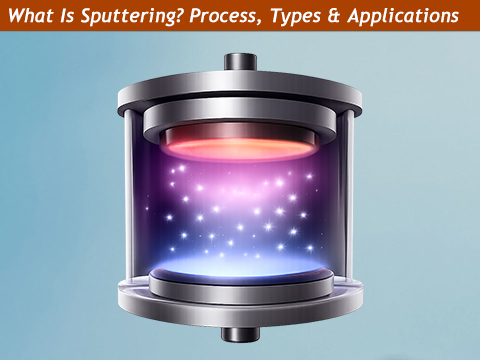
The basic idea behind sputtering is simple: a high-energy plasma is used to remove atoms from the surface of a sputtering target. These atoms then travel through a vacuum chamber and deposit onto a substrate, forming a thin film layer.
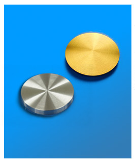
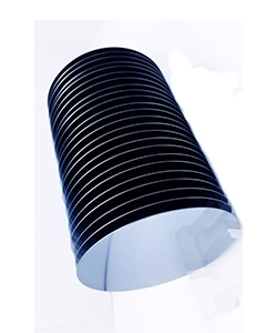
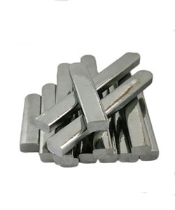
A wide range of materials can be used as sputtering targets, including metals, alloys, and ceramic compounds. Common examples include aluminum, titanium, tantalum, molybdenum, silicon, and ITO targets.
By controlling factors such as target material, gas type, power, and deposition conditions, manufacturers can produce thin films with precise thickness and specific performance characteristics.
In this guide, we will explain what sputtering is, how the sputtering process works, the different types of sputtering technologies, common sputtering target materials, and how to choose a reliable sputtering target supplier.
1. What Is Sputtering?
Sputtering is a thin film deposition process that uses high-energy ions to remove atoms from a solid target material and deposit them onto a substrate. It is one of the most important physical vapor deposition (PVD) methods used to create thin coatings with precise thickness and excellent uniformity.
In a sputtering system, the material being deposited is called a sputtering target. The target can be made from metals, alloys, or ceramic compounds, depending on the required coating properties.
The basic sputtering process includes four main steps:
1. Plasma generationA vacuum chamber is filled with an inert gas, usually argon. An electric field is applied to ionize the gas and create plasma.
2. Ion bombardmentPositively charged gas ions are accelerated toward the negatively charged sputtering target. When these ions hit the target surface, they transfer energy to the target atoms.
3. Target atom ejectionThe impact releases atoms from the target surface. These atoms become free particles that move through the vacuum chamber.
4. Thin film formationThe released atoms reach the substrate surface and gradually build up a thin coating layer.
Unlike simple coating methods that only cover the surface, sputtering allows engineers to precisely control the film thickness, composition, and performance. This makes it suitable for applications where even small differences in coating quality can affect product performance.
Common sputtered films include:
· Metal conductive layers for semiconductor devices
· Transparent conductive coatings such as ITO for displays and solar cells
· Protective coatings for tools and industrial components
· Optical coatings for lenses and precision components
The performance of the final coating depends greatly on the quality of the sputtering target. High-purity targets with consistent composition and density help achieve stable deposition rates and reliable thin film properties.
2. How Does the Sputtering Process Work?
The sputtering process takes place inside a vacuum chamber, where controlled conditions allow atoms to be removed from a target and deposited onto a substrate. Although the technology behind sputtering is advanced, the basic principle is easy to understand: use plasma ions to knock atoms out of a target and build a thin film layer on another surface.
The sputtering process mainly includes the following steps:
Step 1: Creating a Vacuum Environment
Before deposition begins, air is removed from the sputtering chamber to create a high-vacuum environment. This reduces contamination and allows sputtered atoms to travel smoothly from the target to the substrate.A small amount of inert gas, usually argon (Ar), is then introduced into the chamber.
Step 2: Generating Plasma
An electrical voltage is applied between the target and the chamber. The argon gas atoms become ionized, creating a plasma containing positively charged argon ions and free electrons.The plasma provides the energy needed for the sputtering reaction.
Step 3: Bombarding the Sputtering Target
The sputtering target is connected as the negative electrode (cathode). Positively charged argon ions are attracted toward the target surface at high speed.When these ions hit the target, their kinetic energy is transferred to the target material. This impact causes atoms on the target surface to be released.
Step 4: Ejecting Target Atoms
The released target atoms travel through the vacuum chamber as vaporized particles. Since the process does not require melting the material, sputtering can be used for many materials with high melting points, including refractory metals and ceramic compounds.Step 5: Forming the Thin Film
The sputtered atoms reach the substrate surface and gradually accumulate, forming a thin and uniform coating layer.By adjusting deposition parameters such as:
· Plasma power
· Gas pressure
· Target-to-substrate distance
· Deposition time
· Reactive gas ratio
manufacturers can control the film thickness, structure, and properties.
Why Is Sputtering Widely Used?
Sputtering has become a preferred thin film deposition method because it offers several advantages:· Wide material compatibility: Suitable for metals, alloys, semiconductors, and ceramic materials.
· Excellent coating uniformity: Produces consistent films over large substrate areas.
· Strong film adhesion: High-energy particles create strong bonding between the coating and substrate.
· Precise thickness control: Allows deposition of very thin layers from nanometers to micrometers.
· Low substrate temperature: Suitable for heat-sensitive materials.
Because of these advantages, sputtering is widely used in advanced manufacturing, where precise and reliable thin film coatings are required.
3. What Are the Main Types of Sputtering?
There are several sputtering technologies developed for different materials and coating requirements. The most common types include DC sputtering, RF sputtering, magnetron sputtering, and reactive sputtering.
3.1 DC Sputtering
DC sputtering uses a direct current power supply to generate plasma and accelerate ions toward the target surface.Because it works best with conductive materials, it is mainly used for metal targets such as aluminum, copper, and titanium.
Common applications:
· Semiconductor metal layers
· Decorative coatings
· Conductive films
3.2 RF Sputtering
RF sputtering uses radio-frequency power, allowing it to deposit insulating and ceramic materials that are difficult to process with DC sputtering.Common target materials:
· SiO₂
· Al₂O₃
· TiO₂
Common applications:
· Optical coatings
· Semiconductor dielectric layers
· Electronic components
3.3 Magnetron Sputtering
Magnetron sputtering is the most widely used industrial sputtering technology. It uses a magnetic field to increase plasma density near the target surface, improving deposition efficiency and film uniformity.Key advantages:
· Higher deposition rate
· Better coating uniformity
· Improved target utilization
It is widely used in semiconductor, display, solar, and optical coating industries.
3.4 Reactive Sputtering
Reactive sputtering introduces reactive gases such as oxygen or nitrogen during the deposition process to create compound films.Examples:
· Titanium + Nitrogen → TiN
· Aluminum + Oxygen → Al₂O₃
This method is commonly used for producing hard coatings, protective films, and functional materials.
4. How Are Sputtering Targets Manufactured?
The quality of a sputtering target directly affects thin film performance, including coating uniformity, deposition stability, and target lifetime. Different materials require different manufacturing methods to achieve high purity and consistent properties.
The two main manufacturing routes are vacuum melting and powder metallurgy.
Vacuum Melting Route
Vacuum melting is commonly used for metals and alloys that can be melted and cast, such as:· Titanium (Ti)
· Tantalum (Ta)
· Niobium (Nb)
· Zirconium (Zr)
· Nickel (Ni)
The general process includes:
Vacuum melting → Ingot processing → Hot working → CNC machining → Surface finishing → Quality inspection
This process helps achieve high purity, uniform composition, and reliable mechanical properties.
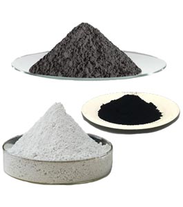
Powder Metallurgy Route
Powder metallurgy is mainly used for materials that are difficult to melt, including refractory metals and ceramic targets such as:· Molybdenum (Mo)
· Tungsten (W)
· ITO
· Oxide targets
The typical process includes:
Powder preparation → Pressing → Sintering → Machining → Inspection
This method improves material density and helps produce targets with stable sputtering performance.
5. What Are the Applications of Sputtering Technology?
Sputtering has become an essential thin film deposition technology across many industries because it can produce coatings with precise thickness, excellent uniformity, and customized properties.
By selecting different sputtering target materials and process conditions, manufacturers can create films with specific electrical, optical, mechanical, or protective functions.
Semiconductor Manufacturing
Sputtering is widely used in semiconductor production to deposit thin metal and compound layers on silicon wafers.Common applications include:
· Conductive interconnect layers
· Barrier layers
· Electrode films
Materials such as aluminum, copper, titanium, and tantalum are commonly used as sputtering targets in semiconductor processes.
Display Technology
In display manufacturing, sputtering is mainly used to create transparent conductive films and functional layers.A typical example is ITO (Indium Tin Oxide) coating, which provides electrical conductivity while maintaining high transparency.
Applications include:
· LCD displays
· Touch screens
· OLED components
Solar Energy
Sputtering plays an important role in thin-film solar cell production by depositing conductive and functional layers.Common target materials include:
· ITO
· AZO
· Molybdenum
· Other metal and compound targets
These coatings help improve electrical performance and energy conversion efficiency.
Optical Coatings
Sputtering is widely used to produce optical films with controlled reflection, transmission, and durability.Applications include:
· Anti-reflective coatings
· Protective optical films
· Filters and precision lenses
Materials such as silicon dioxide, titanium dioxide, and aluminum oxide are commonly used for optical applications.
Protective and Functional Coatings
Sputtering can also improve the surface performance of industrial components by adding thin protective layers.Applications include:
· Wear-resistant coatings
· Corrosion-resistant films
· Decorative coatings
· Tool coatings
Reactive sputtering is often used to produce hard compounds such as titanium nitride (TiN), which provides excellent hardness and wear resistance.
Why Sputtering Is Important for Advanced Manufacturing
The ability to deposit thin, uniform, and high-performance coatings makes sputtering a key technology in modern manufacturing.As industries continue to demand smaller electronic devices, better energy solutions, and more durable materials, sputtering will remain an important method for producing advanced thin films.
6. Sputtering vs Other Thin Film Deposition Methods
Sputtering is one of the most widely used thin film deposition methods, but it is not the only option available. Other technologies, such as evaporation and chemical vapor deposition (CVD), are also commonly used in different applications.
Each method has its own advantages depending on the material, coating requirements, and production conditions.
| Deposition Method | Working Principle | Main Advantages |
|---|---|---|
| Sputtering | Uses plasma ions to eject atoms from a solid target and deposit them onto a substrate | Wide material compatibility, strong film adhesion, good thickness control |
| Evaporation | Uses thermal energy or electron beams to vaporize a source material | Simple process, high deposition rate, suitable for high-purity coatings |
| CVD | Uses chemical reactions between gases to form a coating layer on a substrate | Excellent coating uniformity and ability to coat complex surfaces |
Sputtering vs Evaporation
Both sputtering and evaporation are physical vapor deposition (PVD) methods, but they use different approaches to create the coating material.Evaporation heats the source material until it becomes vapor, while sputtering uses plasma ions to physically remove atoms from a target.
Compared with evaporation, sputtering offers:
· Better adhesion between film and substrate
· More choices of coating materials
· Better control of film composition
· Ability to deposit high melting point materials
For these reasons, sputtering is often preferred for advanced electronic and industrial coating applications.
Sputtering vs CVD
CVD uses chemical reactions between gas molecules and the substrate surface to form a thin film. It is widely used in semiconductor manufacturing where excellent step coverage is required.Compared with CVD, sputtering provides:
· Lower processing temperatures
· A wider range of target materials
· Fewer chemical reaction by-products
· Simpler material switching between different targets
However, CVD may have advantages when coating complex three-dimensional structures or requiring highly conformal films.
Why Choose Sputtering for Thin Film Deposition?
Sputtering is often selected when manufacturers need:· High-quality and uniform thin films
· Strong coating adhesion
· Precise thickness control
· Flexible material selection
· Stable large-area coating performance
By choosing the appropriate sputtering system and target material, manufacturers can achieve reliable coatings for applications ranging from semiconductor devices to optical components and industrial products.
7. How to Choose a Reliable Sputtering Target Supplier?
The quality of a sputtering target directly affects coating performance, deposition stability, and production efficiency. Choosing the right sputtering target supplier helps ensure consistent thin film quality.
When selecting a supplier, consider the following factors:
Material Quality
High-purity materials and consistent composition are essential for stable sputtering performance. A reliable supplier should provide strict material control and inspection reports.Manufacturing Capability
Different materials require different production methods. An experienced sputtering target manufacturer should have capabilities in:· Vacuum melting
· Powder metallurgy
· Precision machining
· Target bonding
Quality Control
Proper testing helps ensure target reliability, including:· Chemical composition analysis
· Density testing
· Microstructure inspection
· Surface quality checks
Customization Support
A professional supplier should provide customized solutions, including different target shapes, sizes, materials, and bonding options.Choosing a reliable sputtering target partner ensures stable deposition performance and supports long-term production needs.
Conclusion
Sputtering is more than a coating process. It is a precise material engineering technology that allows manufacturers to control surface properties at the microscopic level.
The performance of a thin film depends on many factors, from the sputtering process to the quality and consistency of the target material. A well-designed deposition solution can improve product reliability, efficiency, and performance across different industries.
As advanced technologies continue to demand thinner, smarter, and more functional coatings, sputtering will remain an important solution for next-generation manufacturing.
Looking for a reliable sputtering target manufacturer? AEM Deposition provides high-purity metal, alloy, and ceramic sputtering targets with customized solutions for various thin film deposition applications.
LATEST NEWS