Brief Introduction of DC Sputtering
views, Updated: 2021-09-24
Direct Current (DC) Sputtering is a Thin-film Physical Vapor Deposition (PVD) Coating technique where a target material to be used as the coating is bombarded with ionized gas molecules causing atoms to be “Sputtered” off into the plasma. These vaporized atoms are then deposited when they condense as a thin-film on the substrate to be coated. DC Sputtering is the most basic and inexpensive type of sputtering for PVD metal deposition and electrically conductive target coating materials. One major advantage of DC as a power source for this process is that it is easy to control and is a low-cost option if you are doing metal deposition for coating. DC Sputtering is used extensively in the semiconductor industry, creating microchip circuitry on the molecular level. It is used for gold sputter coatings of jewelry, watches, and other decorative finishes, for non-reflective coatings on glass and optical components, as well as for metalized packaging plastics.
DC Magnetron Sputtering Process
A DC Sputtering coating system's basic configuration is the target material to be used as a coating is placed in a vacuum chamber parallel to the substrate to be coated.
The vacuum chamber is evacuated to a base pressure removing H2O, Air, H2, Ar and then backfilled with a high purity inert process gas. Usually, Argon is used due to its relative mass and ability to convey kinetic energy upon impact during high energy molecular collisions in the plasma that creates the gas ions that are the primary driving force of sputter thin-film deposition.
A DC electrical current typically in the -2 to -5 kV range is then applied to the target coating material called the cathode or point at which electrons enter the system known as the negative bias. A positive charge is also applied to the substrate to be coated, which becomes the anode.
The electrically neutral argon gas atoms are first ionized as a result of the forceful collision of these gas atoms onto the surface of the negatively charged target, which eject atoms off into the plasma – a hot gas‐like state consisting of roughly half gas ions and half electrons that emits the visible plasma glow.
The ionized argon gas atoms are then driven to the substrate, which is the anode or positively charged bias attracting ionized gas ions, electrons, and the vaporized target coating atoms, which condense and form a thin-film coating on the substrate to be coated. DC Magnetron sputtering uses magnets behind the negative cathode to trap electrons over the negatively charged target material. They are not free to bombard the substrate, allowing for faster deposition rates.
The Limitation of DC Sputtering
The magnetic field forms a boundary "tunnel" that traps electrons near the target's surface that improves the efficiency of the gas ion formation. DC Magnetron Sputtering allows for a higher current at lower gas pressure that achieves an even higher thin-film deposition rate.
While DC Sputtering is the economical solution of choice for many types of metal coatings, its primary limitation is that non-conducting dielectric insulating materials take on a charge over time, which can result in quality issues like arcing or the poisoning of the target material with a charge that can result in the complete cessation of sputtering.
Several more complicated technologies have been developed to overcome these limitations of DC Sputtering, such as Radio Frequency (RF) Sputtering and HIPIMS or High Power Impulse Magnetron Sputtering. RF Sputtering alternates the electrical charge at radio frequency to prevent a charge buildup on the target or coating material. HIPIMS utilizes a very high voltage, short-duration burst of energy focused on the target coating material to generate a high-density plasma that results in a high degree of ionization of the coating material in the plasma.
Despite the relative simplicity of DC Sputtering, it usually has low deposition rates compared to more complicated HIPIMS resulting from lower plasma densities and higher gas densities.
However, the relative simplicity of the DC Power source compared to RF or HIPMIS Power sources require much more complicated configuration, cabling, and higher energy costs. It continues to make DC Sputtering the low-cost solution for many types of vacuum metal deposition like gold sputtering and other electrically conductive coatings.
Thin Film Deposition Materials
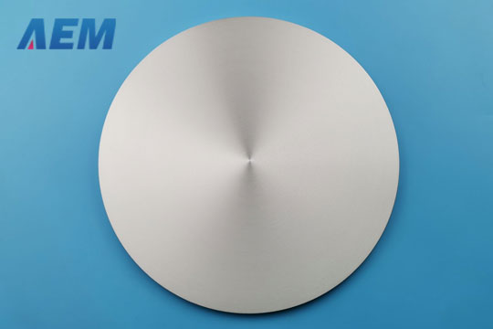
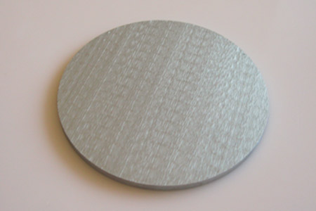
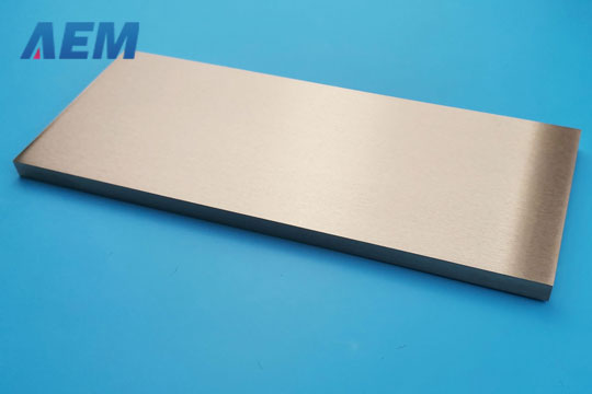
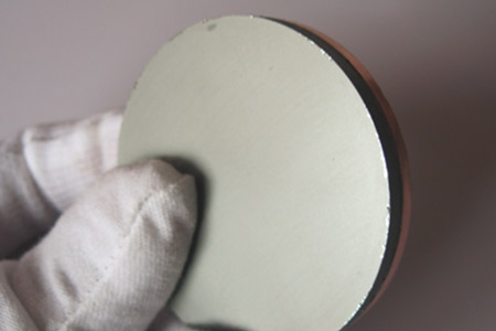
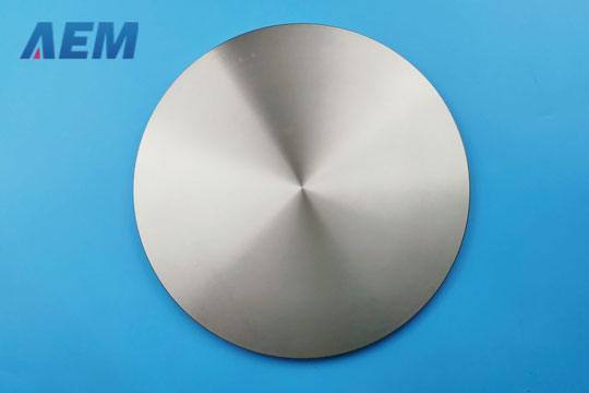
Thin-film deposition materials include but are not limited to sputtering targets and evaporation materials. For more information on types of thin-film coating deposition, please pay sustained attention to AEM Deposition. By the way, AEM Deposition also is an excellent thin-film deposition materials supplier. We provide high-quality sputtering targets (target bonding services also offer), evaporation materials, and other thin-film coating deposition materials.
LATEST NEWS
2025-05-29
2025-05-22
2025-05-09
2025-04-09
2025-04-09


 +86-731-89578196
 [email protected]