+86-731-89578196
 [email protected]

- Home
- Our Company
-
Products
Sputtering Targets

- Industries
- Blog
- FAQ
- Contact Us


Essential Basics of Thin Film Deposition By Sputtering
views, Updated: 2021-09-24
There are several methods of Thin-film Deposition, which is a vacuum technology for applying coatings of pure materials to the surface of various objects. The coatings are usually in the thickness range of angstroms to microns and can be a single material or multiple materials in a layered structure. The object to be coated is referred to as the substrate & wafers and can be any of a wide variety of things such as semiconductor wafers, solar cells, optical components, or many other possibilities. The materials to be applied can be pure atomic elements, including metals and non-metals, or molecules such as oxides and nitrides.
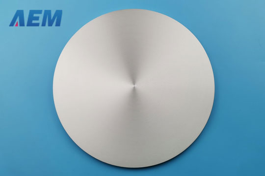
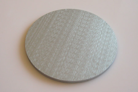
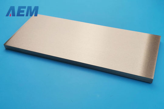
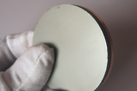
One technique is called Sputtering. The sputtering method of thin-film deposition involves introducing a controlled gas, usually chemically inert argon, into a vacuum chamber and electrically energizing a cathode to establish a self-sustaining plasma. The cathode's exposed surface, called the target, is a slab of the material to be coated onto the substrates. The gas atoms lose electrons inside the plasma to become positively charged ions, which are then accelerated into the target and strike with sufficient kinetic energy to dislodge atoms or molecules of the target material. It can be thought of as a sort of atomic-scale bead blasting. This sputtered material now constitutes a vapor stream, which traverses the chamber and hits the substrate, sticking to it as a coating or "thin-film".
To get good film adhesion, it is, of course, necessary for the substrate surface to be clean. Appropriate cleaning and handling steps must be employed before placing substrates into the vacuum chamber. It is also not uncommon to also have optional in situ cleaning features such as sputter etch incorporated into the sputter system. Steps may have to be taken to control various film properties as desired. Fortunately, sputter system design can allow adjustability of several parameters to give process engineers the ability to achieve desired results for such variables as thickness, uniformity, adhesion strength, stress, grain structure, optical or electrical properties. There are also considerations, such as what type of power to use on the cathodes. DC power is suitable for conductive materials, but RF power can also sputter non-conductive materials. Pulsed DC has advantages for some processes, such as reactive sputtering.
Another process option is Reactive Sputtering, which utilizes a non-inert gas, such as oxygen, combined with an elemental target material, such as silicon. This gas creates a chemical reaction with the sputtered atoms inside the chamber, forming a new compound that becomes the coating instead of the original pure target material.
Thin-film Deposition Sputter systems can also be configured with various hardware or software options. These can include sputter etch or ion source capability for in situ cleanings of substrate surfaces or substrate preheat stations. Other options can include multiple cathodes, confocal arrangements of cathodes, load lock stations and/or substrate handlers, and substrate bias capability.
Thin-film Deposition Sputtering offers the advantages of film adhesion strength and good step or via coverage in its various forms. It is also possible to perform simultaneous double-sided coating with appropriate mechanical configuration, and load lock chamber entry and exit are commonly available.
Thin Film Deposition Materials
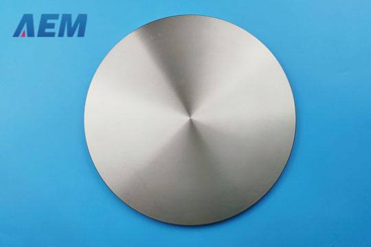
Thin-film deposition materials include but are not limited to sputtering targets and evaporation materials. For more information on types of thin-film coating deposition, please pay sustained attention to AEM Deposition. By the way, AEM Deposition also is an excellent thin-film deposition materials supplier. We provide high-quality sputtering targets (target bonding services also offer), evaporation materials, and other thin-film coating deposition materials.
LATEST NEWS