


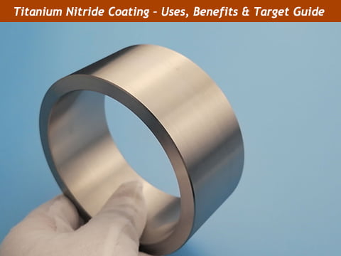
Titanium Nitride Coating: Applications, Benefits & Target Solutions
Date: 2025-12-19
Abstract: Explore titanium nitride coating applications, benefits, and how high-purity titanium sputtering targets from AEM Deposition improve coating quality and performance.
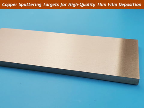
Copper Sputtering Targets: High-Performance Solutions for Thin Film Deposition
Date: 2025-12-12
Abstract: Discover the benefits of copper sputtering targets for thin-film deposition. Learn how to purchase high-quality copper targets and more.
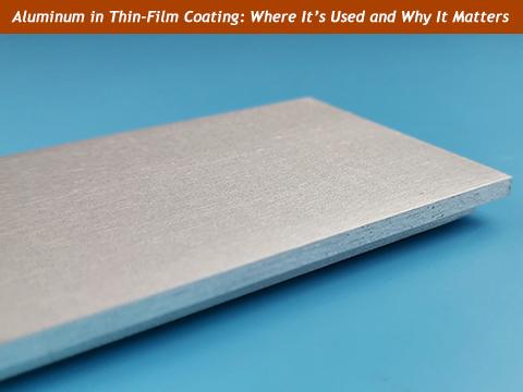
Aluminum in Thin-Film Coating: Where It's Used and Why It Matters
Date: 2025-12-11
Abstract: Discover where aluminum thin films are used, their key benefits, and how to choose the right sputtering target for semiconductors, displays, and energy devices.
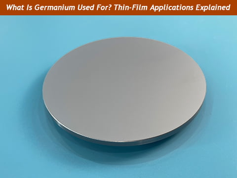
What Is Germanium Used For? Thin-Film Applications Explained
Date: 2025-12-09
Abstract: Discover how germanium is used in infrared optics, semiconductors, and solar cells. AEM Deposition supplies custom high-purity germanium targets worldwide.
Choosing the Right Silicon Sputtering Target: Grades, Specs & Buying Tips
Date: 2025-12-08
Abstract: Learn how to choose the right silicon sputtering target by comparing grades, specs, and applications. Expert tips for selecting the right supplier.
Aluminum Sputtering Targets: Properties, Grades, and Performance in Thin-Film Coating
Date: 2025-12-08
Abstract: Learn about aluminum sputtering targets, including purity grades (4N–5N5), alloy options, properties, and how to choose the right target for thin-film coating.
Bismuth Uses: Where This Unique Metal Matters Today
Date: 2025-11-28
Abstract: Explore the key uses of bismuth across major industries. Learn its essential properties, why it performs well in thin-film coatings, and how AEM Deposition supplies high-purity bismuth materials.
ITO Coating: Transparent Conductive Films Explained
Date: 2025-11-06
Abstract: Discover how ITO coating combines transparency and conductivity for displays, solar panels, and smart glass. Learn its process, uses, and materials.
Ceramic Refractory Materials: Properties, Types, and Applications in Thin-Film Coating
Date: 2025-10-24
Abstract: Learn about ceramic refractory materials — their key properties, types, and applications in thin-film coating and advanced material industries.
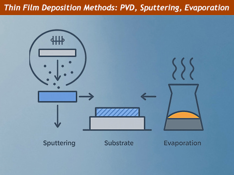
Thin Film Deposition Methods Explained: PVD, Sputtering, Evaporation
Date: 2025-08-08
Abstract: Discover key thin film deposition methods, including PVD, sputtering, and evaporation. Learn how each works, their benefits, and the best uses for your coatings.
Evaporation Deposition Guide: Processes, Types, and Materials
Date: 2025-06-20
Abstract: Learn the essentials of evaporation deposition with expert tips for material buyers—covering processes, materials, techniques, and applications.
Sputter Coating Explained: Key Benefits, Applications & Target Solutions
Date: 2025-06-20
Abstract: Learn what sputter coating is, how it works, key benefits, and how AEM Deposition provides high-quality sputtering targets for advanced thin-film coatings.