


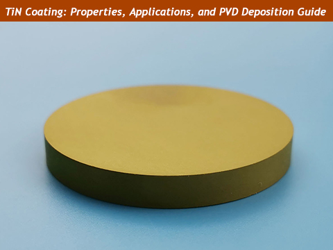
TiN Coating: Properties, Applications, and PVD Deposition Guide
Date: 2026-07-21
Abstract: Learn about TiN coating properties, PVD deposition methods, applications, and how TiN sputtering targets help achieve high-quality coatings.
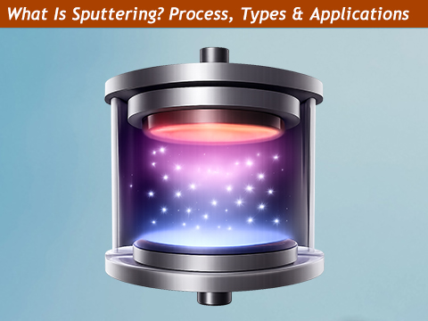
What Is Sputtering? A Complete Guide to Thin Film Deposition
Date: 2026-07-17
Abstract: Learn what sputtering is, how the sputtering process works, its main types, applications, and how sputtering targets support thin film deposition.
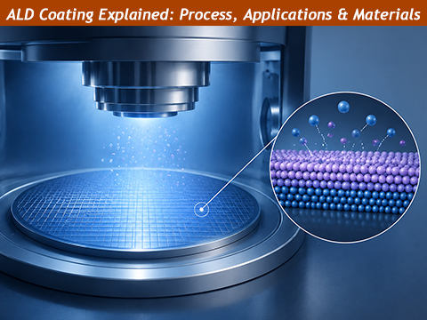
ALD Coating Explained: Process, Applications, and Materials for Advanced Thin Films
Date: 2026-07-09
Abstract: Learn what ALD coating is, how Atomic Layer Deposition works, its key advantages, applications, and materials for advanced thin films.
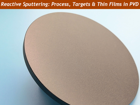
Reactive Sputtering: From Metal Targets to Compound Thin Films in PVD Systems
Date: 2026-06-30
Abstract: Learn reactive sputtering in PVD systems, including process principles, metal targets, compound film formation, and industrial applications.
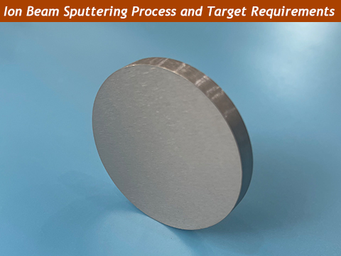
Ion Beam Sputtering Process and Target Material Requirements
Date: 2026-06-23
Abstract: Learn how ion beam sputtering works, key target material requirements, common target materials, and applications in thin-film deposition.
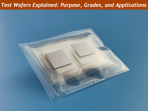
Test Wafers Explained: Purpose, Grades, and Applications
Date: 2026-06-16
Abstract: Discover the purpose of test wafers, how they differ from other wafer grades, and where they are used in semiconductor manufacturing.
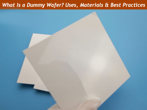
What Is a Dummy Wafer? Functions, Uses, Materials, and Best Practices
Date: 2026-06-12
Abstract: Discover the purpose of dummy wafers, their applications, material considerations, and management tips for efficient semiconductor processes.
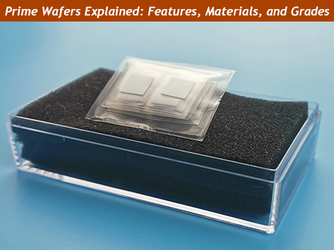
What Are Prime Wafers? A Guide to Semiconductor-Grade Wafers
Date: 2026-06-04
Abstract: Learn what prime wafers are, including their features, materials, grades, and applications in semiconductor manufacturing.
Indium Tin Oxide (ITO): Key Features, Products, Manufacturing Process, and Applications
Date: 2026-04-22
Abstract: Discover ITO (Indium Tin Oxide), its features, main products for thin-film coatings, manufacturing process, and its applications.
DLC Coatings Explained & How to Choose the Right Sputtering Target
Date: 2026-04-16
Abstract: Learn how DLC coatings work and how to choose the right sputtering target. AEM Deposition offers premium targets for durable, high-performance coatings.
Choosing the Right Sputtering Targets for Conductive Coatings
Date: 2026-04-15
Abstract: Learn how to choose the right sputtering targets for high-quality conductive coatings. Explore materials, applications, and next-gen options.
Germanium Applications: Key Uses in Electronics, Optics, and Thin Film Technologies
Date: 2026-03-20
Abstract: Learn germanium applications in fiber optics, infrared optics, semiconductors, and solar cells. Includes germanium wafers and germanium sputtering targets.