


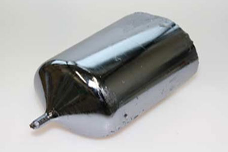
Gallium Arsenide Crystal (GaAs)
Gallium Arsenide Crystal
Gallium Arsenide (GaAs) has high electron mobility. The GaAs substrate is commonly applied in light-emitting diodes, laser diodes, photovoltaic devices, high electron mobility transistors, and heterojunction bipolar transistors.
Gallium Arsenide Crystal Physical Properties
| Material | GaAs |
|---|---|
| Growth Method | VGF |
| Lattice (A) | a=5.653 |
| Structure | M3 |
| Melting Point | 1238℃ |
| Density(g/cm3) | 5.31 g/cm3 |
| Doped Material | Si-doped / Zn-doped/ Undoped |
| Type | N-type/P-type/ Semi-insulating |
| Carrier Concentration (cm-3) | 5 x 10¹⁷ |
| EPD (Average) | <5 x 10⁵/cm2 |
Gallium Arsenide Crystal Specifications
| Size | 25mmx25mm, 10mmx10mm, 10mmx5mm, 5mmx5mm |
|---|---|
| Thickness | 350um |
| Polished | SSP or DSP |
| Orientation | <100>,<110>, <111> |
| Redirection Precision | ±0.5° |
| Angle of Crystalline | Special size and orientation are available on demand. |
| Surface Roughness (Ra:) | <5Å |
Gallium Arsenide Crystal Package
Packaged with class 100 clean bag in a class 1000 clean room.
Related Products of Gallium Arsenide Crystal
|
Semiconductor Crystals |
Scintillation Crystals |
Photoelectric Crystals |
|
Infrared Crystals |
Laser Crystals |
Nonlinear Optical Crystals |
FREE QUOTE
 Click to download datasheet about Gallium Arsenide Crystal (GaAs)
 Unable to find the required data sheet? Click here to send an email and get it.
 Click here to get answers to Frequently Asked Questions (FAQ).