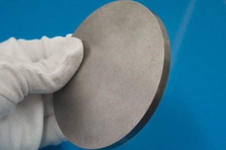
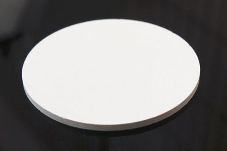
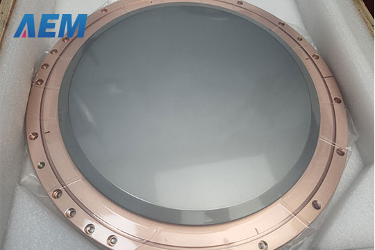
Titanium Sputtering Targets (Ti)
| Material Type | Titanium |
| Symbol | Ti |
| Atomic Weight | 47.867 |
| Atomic Number | 22 |
| Color/Appearance | Silvery Metallic |
| Thermal Conductivity | 21.9 W/m.K |
| Melting Point (°C) | 1,660 |
| Coefficient of Thermal Expansion | 8.6 x 10⁻⁶/K |
| Theoretical Density (g/cc) | 4.5 |
| Z Ratio | 0.628 |
| Sputter | DC |
|
Max Power Density* (Watts/Square Inch) |
50 |
| Type of Bond | Indium, Elastomer |
| Comments | Alloys with W/Ta/Mo; evolves gas on first heating. |
What are Titanium Sputtering Targets
In order to better understand titanium sputtering targets, it is first important to understand titanium.
Titanium is a metallic element that is known for its strength and durability. The relatively high melting point (more than 1,650℃ or 3,000℉ ) makes it useful as a refractory metal. Titanium sputtering targets are made from titanium metal and are used in a process called sputter coating.
The titanium targets are commonly used in hardware tool coating, decorative coating, semiconductor components, and flat display coating. There are two main methods for making titanium sputtering targets: melting and casting.
Melting: the metal is heated to a high temperature until it becomes liquid. It is then poured into a mold and allowed to cool, resulting in a solidified target.
Casting: the metal is placed in a vacuum chamber and bombarded with high-energy particles. This causes the metal to vaporize, and as it cools, it condenses onto the surface of the target.
It is one of the core materials for preparing integrated circuits, and purity usually requires over 99.99%. AEM offers Titanium alloy targets such as Tungsten Titanium (W/Ti 90/10 wt%) Sputtering Target, an essential material for the semiconductor and solar industry. The W/Ti sputtering target density can reach over 14.24 g/cm3, and the purity can reach 99.995%.
Titanium Sputtering Targets Specification
Titanium Sputtering Targets
Purity: 99.9-99.999%
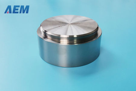
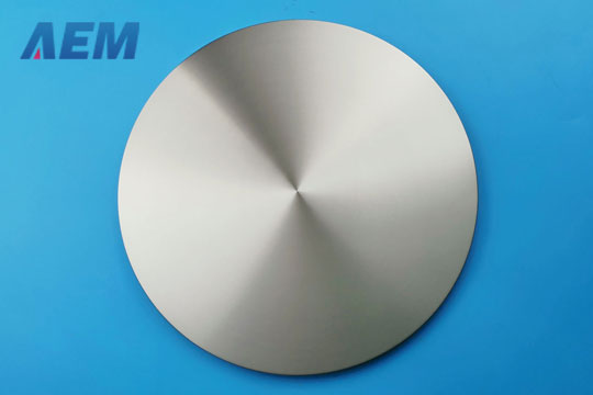
Circular: Diameter <= 14 inch, Thickness >= 1mm
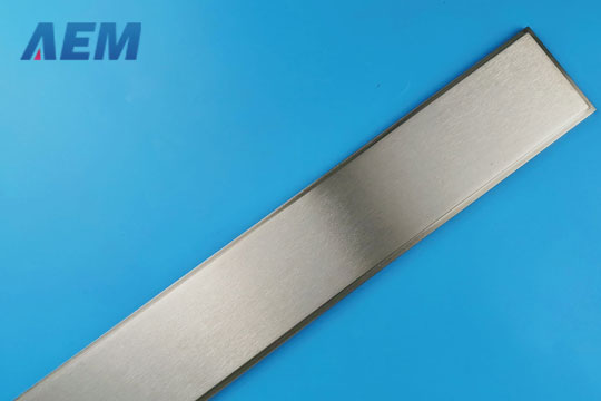
Block: Length <= 32 inch, Width <= 12 inch, Thickness >= 1mm
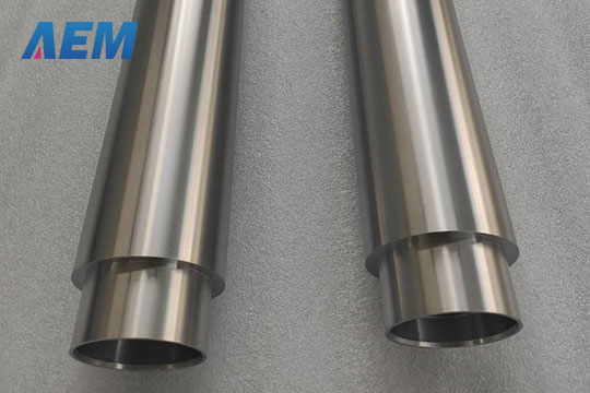
Targets Type: Planar sputtering target, Rotary sputtering target
If you're looking for Titanium sputtering targets, we'll work with you to find the best solution for your needs.
Titanium Sputtering Targets Analysis
More Information on Titanium Sputtering Targets
Applications• Decorative coating• Hardware tool coating • Semiconductor • Flat panel displays |
Features• Competitive pricing• High purity • Grain refined, Engineered microstructure (average grain size < 20 um) • Semiconductor grade |
Manufacturing Process• Melting (EB-Electron Beam Melting)• Analysis • Casting & Grain refinement Forging, Rolling, Annealing, Micrography, Machining • Cleaning and final packaging - Cleaned for use in vacuum Protection from environmental contaminants Protection during shipment |
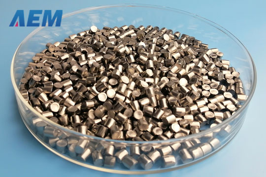
Options• 99.9% minimum purity• Semiconductor grade titanium alloys available Ti/Al, W/Ti 90/10 wt%) • Smaller sizes also available for R&D applications • Sputtering target bonding service |
Related Products of Titanium Sputtering Targets
 Click to download datasheet about Titanium Sputtering Targets (Ti)
 Unable to find the required data sheet? Click here to send an email and get it.
 Click here to get answers to Frequently Asked Questions (FAQ).