+86-731-89578196
 [email protected]

- Home
- Our Company
-
Products
Sputtering Targets

- Industries
- Blog
- FAQ
- Contact Us


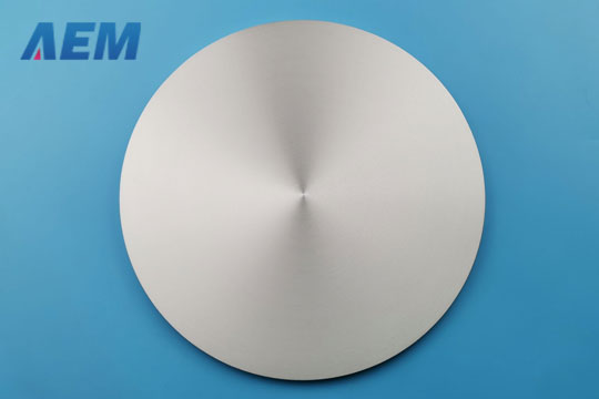
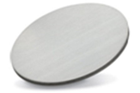
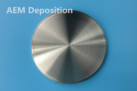
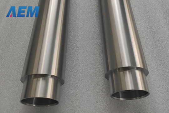
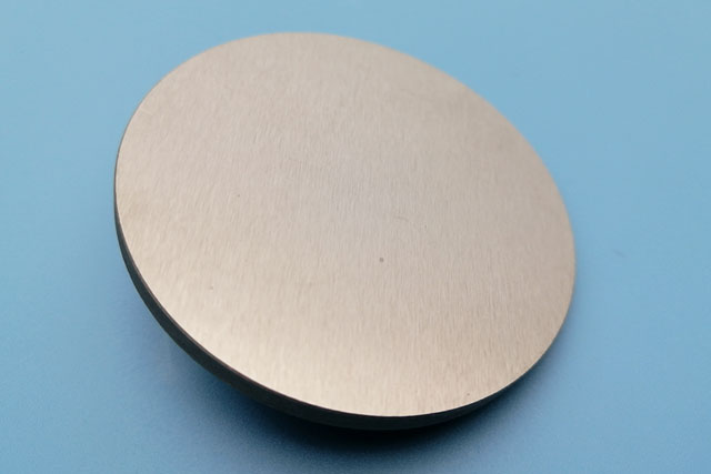
Semiconductor Sputtering Targets
views, Updated: 2021-09-24
Sputtering targets must meet stricter standards for high-quality ever to produce sub-micron scale and wafer targets in ever-larger sizes.
- Low particle
- Good film uniformity
- High usage efficiency
Features of Semiconductor Sputtering Targets
- Low-particle targets
- ULVAC has developed sputtering targets that suppress the generation of particles that can be the source of problems in the sputtering process.
- Gaseous elements are one factor in causing particle emissions, especially in aluminum targets. We are working to lower emissions by utilizing a vacuum melting method for refining and ingot purification processes.
- Attaining high uniformity by adjusting the metal microstructure
- ULVAC uses manufacturing processes that ensure high uniformity and a fine metal microstructure in most of its targets for semiconductor products, including high purity cobalt targets and titanium targets.
- Utilizing a fine metal microstructure with a high degree of uniformity allows uniform magnetic flux leakage on the target surface of high purity cobalt targets.
- Meticulous quality control system
- Integrated process manufacturing at ULVAC takes product characteristics and contours into account during production. Sophisticated analysis/evaluation system such as the GD-MS (glow discharge mass spectrometer) ensures purity and a high level of quality.
Sputtering Targets for Semiconductors
| Application Field | Materials | Manufacturing Method | Purpose of Use |
| Electrode Materials | W (5N) | Powder sintering | Gate area |
| Co(5N) | Melting method | Gate area | |
| Ni(5N) | Melting method | Gate area | |
| Ti(5N) | Melting method | Lynear, Barrier etc. | |
| Various silicide(4N up) | Powder sintering | ||
| Wiring Materials | Al(5N, 5N5) & Al alloy such as AlCu(5N, 5N5) | Vacuum melting method | Inter conect |
| Cu(6N) | Melting method | Inter conect | |
| Compound Semiconductor Materials | Au, Au alloy(4N) | Melting method | Wiring |
| WSi(5N) | Powder sintering | Electrode | |
| SiO2(4N,6N) | Artificial/ natural quartz | Insulating material | |
| Mounting & Wiring | Al(5N, 5N5)& Al alloy(5N, 5N5) | Vacuum melting method | Wiring |
| Cu(4N) | Melting method | Wiring | |
| Cr(3N) | Powder sintering | Barriers | |
| Precious metal materials | Melting method | Wiring | |
| TiW(4N up) | Powder sintering | Barriers | |
| Ni(4N) | Melting method | Barriers | |
| Capacitor Materials | BST | Powder sintering | DRAM/thin film capacitors |
| PZT | Powder sintering | FeRAM | |
| Barrier Materials | Ti(4N5) | Melting method | |
| TiW(4N up) | Powder sintering |
Target Material for Mainstream 300mm Wafers
| Target Material | Al-0.5mass%Cu | Ti | Cu | Ta | W |
| Purity | 5N5up (Low-U, Th specifications) | 4N5up | 6Nup | 6Nup (Except for Nb and W) | 5N |
| Backing Plate Material | Aluminum or copper alloy | Aluminum alloy | Aluminum alloy | Aluminum or copper alloy |
Aluminum alloy or copper alloy |
| Bonding Method |
Electron beam welding, integrated part structure, or metal bonding |
Diffusion bonding | Diffusion bonding | Diffusion bonding | Metal bonding |
LATEST NEWS