


Sputtering Targets
Evaporation Materials
Evaporation Sources
High Purity Materials
Thin Film Substrates
Crytstal Materials


 +86-731-89578196
 [email protected]
Sputtering Targets


At AEM, we proudly offer high-quality thermal oxide silicon wafers, produced with advanced manufacturing techniques to ensure superior precision and durability. Our thermal oxide silicon wafers provide excellent surface properties, making them reliable for high-performance needs.
As an industry leader, AEM excels in delivering customizable solutions, backed by strong technical support and a commitment to excellence. With AEM, you can trust in our expertise and dedication to providing top-tier wafers for your most demanding projects.
| Size | 10x10, 15x15, 20x 15, 20x 20 (customized sizes are available) |
|---|---|
| Dia 1'', Dia 2'',Dia 3'', Dia 4'', Dia 5'' Dia 6'', Dia 8''. Dia12'' | |
| Thickness | 0.3- 0.5mm, 1.0mm |
| Polished | SSP or DSP |
| Orientation | <100>,<110>, <111> |
| Redirection Precision | ±0.5° |
| Redirection the Edge | 2°(special in 1°) |
| Material | Si+SiO₂ | ||
|---|---|---|---|
| Structure | M3 | ||
| Melting Point | 1420℃ | ||
| Density(g/cm3) | 2.4 g/cm3 | ||
| Doped Material | undoped | B-doped | P-doped |
| Type | P /N | P | N |
| Resistivity | >1000 Ωcm | 10-3 ~40 Ωcm | 0.05~0.1 Ωcm |
| Thermal-expans | ≤100/cm2 | ≤100/cm2 | ≤100/cm2 |
| Oxide Thickness | 300~ 500nm (customized sizes are available. | ||
Our wafers are manufactured with the highest precision, ensuring consistent quality and uniformity for every batch.
Featuring excellent thermal oxide layers, our SiO₂ wafers offer enhanced surface characteristics for reliable and stable performance.
We provide tailored solutions to meet your specific wafer thickness, oxide layer, and size requirements, ensuring you get the perfect product for your needs.
Each wafer undergoes rigorous testing and inspection to guarantee top-tier quality, ensuring reliability and performance in critical processes.
We pride ourselves on offering fast and reliable delivery, ensuring your wafers arrive on time, every time.
High-quality silicon wafers are selected and polished to achieve a smooth, defect-free surface, which is essential for uniform oxide growth.
The wafers undergo a thorough cleaning process to remove contaminants, using methods like ultrasonic cleaning and chemical solvents to ensure a pristine surface.
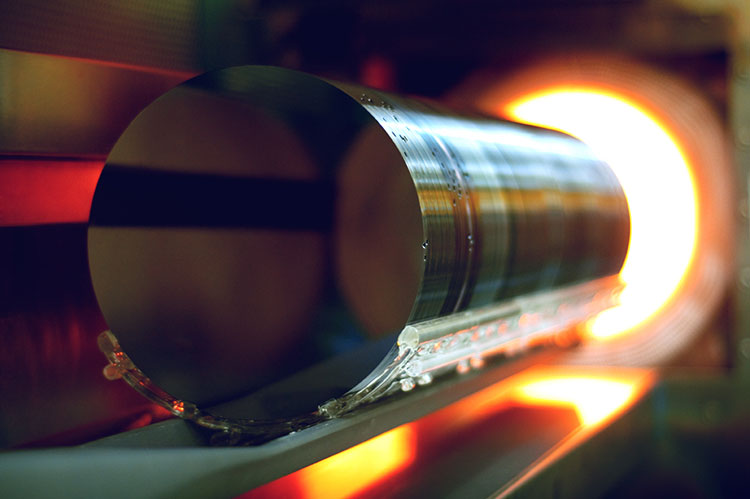
The cleaned silicon wafers are subjected to thermal oxidation, which can be done using either:
The oxidation process is closely monitored to achieve the desired oxide thickness, which can be adjusted by varying the temperature and duration of exposure.
After oxidation, the wafers are gradually cooled to room temperature. Post-oxidation treatments, such as annealing, may be performed to enhance oxide quality.
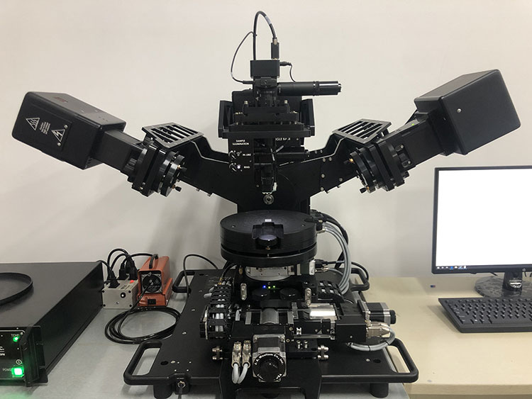
The wafers undergo various characterization techniques, including ellipsometry, to measure oxide thickness and ensure compliance with specifications. Additional tests for electrical and physical properties may also be conducted.
The wafers are cleaned again to eliminate any oxidation byproducts and then packaged in a controlled environment to prevent contamination before shipping.

The thermally grown silicon dioxide (SiO₂) layer provides excellent electrical insulation, making it ideal for isolating different components in integrated circuits, MEMS devices, and power electronics.

Thermal oxide layers effectively reduce surface states that can trap charge carriers, enhancing the performance and stability of semiconductor devices by minimizing electron recombination.

The oxidation process allows for precise control over the oxide layer thickness, ranging from a few nanometers to micrometers, tailored to specific applications like gate oxides or diffusion barriers.

Thermal oxidation results in highly uniform oxide layers across the entire wafer, ensuring consistent performance in large-scale production, particularly in IC fabrication and MEMS.

The oxide layer grown through thermal processes exhibits excellent thermal stability, making it suitable for applications requiring high-temperature processing or operation, such as power devices and optoelectronics.

Thermal oxide silicon wafers have a lower defect density compared to other oxide growth methods, resulting in higher reliability and performance in critical applications, especially in radiation-hard environments.

The SiO₂ layer offers resistance to environmental degradation, such as oxidation or contamination, protecting the wafer surface during various fabrication processes.
Thermal oxide silicon wafers provide electrical isolation and structural integrity in MEMS devices, supporting the integration of mechanical components with electronic systems in applications such as sensors and actuators.
In high-voltage power devices, thermally grown oxide provides dielectric isolation, ensuring efficient and safe operation in power conversion systems, automotive electronics, and energy distribution.

Packaged with class 100 clean bag or wafer container in a class 1000 clean room.
A thermal oxide silicon wafer is a silicon wafer that has a layer of silicon dioxide (SiO₂) grown on its surface through a thermal oxidation process. This oxide layer provides electrical insulation, surface passivation, and other beneficial properties for semiconductor applications.
Wet Oxidation produces a thicker oxide layer more quickly and is ideal for applications that require a larger oxide thickness. Dry Oxidation results in a thinner, higher-quality oxide with better electrical properties, often used in applications requiring precision and reliability, like gate oxides.
Yes, the thickness of the oxide layer, wafer size, and doping levels can be customized to meet the specific requirements of different applications, such as ICs, MEMS, or sensors.
In some cases, thermal oxide wafers can be reclaimed by stripping the oxide layer using an etchant (such as hydrofluoric acid) and then reprocessing the wafer. However, reclaimed wafers may not meet the same quality standards as newly manufactured wafers and are typically used for non-critical applications.
To maintain the quality of thermal oxide silicon wafers, they should be stored in a cleanroom environment with controlled temperature and humidity. Proper wafer handling practices, such as using clean gloves and anti-static storage containers, are also important to avoid contamination or damage to the oxide layer.
Yes, thermal oxide silicon wafers are widely used in research and development (R&D) for testing new semiconductor technologies, creating experimental devices, and developing next-generation ICs. Their precision and high-quality oxide layers make them ideal for prototyping and testing in labs and academic settings.
Yes, thermal oxide silicon wafers can be combined with other types of oxide coatings, such as PECVD (plasma-enhanced chemical vapor deposition) oxide or LPCVD (low-pressure chemical vapor deposition) oxide, depending on the application. This allows for tailored multi-layer structures with different electrical, mechanical, and chemical properties.
Thermal oxide is known for its excellent dielectric properties, low leakage current, and strong silicon interface, making it highly reliable for semiconductor devices. While other dielectric materials like silicon nitride or high-k dielectrics may offer unique benefits for specific applications, thermal oxide remains the most widely used due to its stable performance, mature manufacturing process, and cost-effectiveness.
A sacrificial oxide layer is often grown and then removed to clean the surface of the silicon wafer. This helps eliminate contaminants and defects that may have formed during earlier processing steps, ensuring that the final thermal oxide layer has high purity and excellent electrical properties.
Please be advised that customised specification thermal oxide silicon wafers require approximately 3-4 weeks for shipping. If the order is for a regular specification and we have stock, it can be shipped in 1-2 weeks. Please also understand that if transportation volume accumulates during holidays, the delivery time may be slower.
| Superconducting Substrates | |
| Magnetic Ferroelectricity Substrates | |
| Semiconductor Wafers | |
| GaN Thin Film Substrates | |
| Halide Substrates | |
| Ceramic Substrates | |
| Metal Substrates |