Sputtering Targets
Evaporation Materials
Evaporation Sources
High Purity Materials
Thin Film Substrates
Crytstal Materials


 +86-731-89578196
 [email protected]
Sputtering Targets

| Size | 10x3, 10x5, 10x10, 15x15, 20x15, 20x20,Dia15, Dia 20, Dia 1'' |
|---|---|
| Thickness | 0.5 mm, 1.0 mm |
| Polished | SSP or DSP |
| Crystallographic D spacing | (1120 ) - a plane: 2.379 Å (1102) - r plane: 1.740 Å |
| (1010) - m plane: 1.375 Š(1123) - n plane: 1.147 ů | |
| (0001) - c plane: 2.165 Å (1011) - s plane: 1.961 Å | |
| Redirection Precision | ±0.5° |
| Redirection the Edge | 2°(special in 1°) |
| Angle of Crystalline | Special size and orientation are available on demand. |
| Ra: | ≤5Å(5µm×5µm) |
| Material | Al2O3 |
|---|---|
| Crystal Structure | Hexagonal |
| Lattice (A) | a=4.758, c=12.992 |
| Crystal Purity | >99.99% |
| Density(g/cm3) | 3.98 g/cm3 |
| Melting Point | 2040℃ |
| Hardness | 9.0 (Mohns) |
| Thermal Expansion | 7.5 (x 10-6/℃) |
| Thermal Conductivity | 46.06 @ 0 oC 25.12 @ 100 oC, 12.56 @ 400 oC ( W/(m.K) ) |
| Dielectric Constants | 9.4 @300K at A axis ~ 11.58@ 300K at C axis |
| Loss Tangent at 10 GHz | < 2x10⁻⁵ at A axis , <5 x10⁻⁵ at C axis |
We adhere to stringent quality control processes, ensuring that each sapphire wafer meets the highest standards of performance, durability, and consistency.
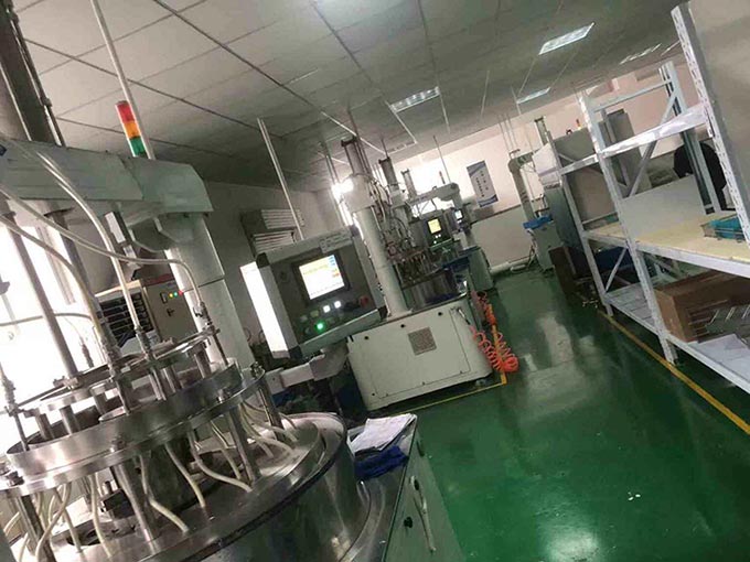
Utilizing state-of-the-art equipment, we guarantee precision and accuracy throughout the entire production process, resulting in wafers that meet exact specifications.
Whether you need specific sizes, thicknesses, or surface finishes, we offer tailored solutions to match your unique requirements.
With a streamlined supply chain, we ensure prompt delivery to keep your project on schedule.
Our knowledgeable team offers personalized assistance and technical advice, guiding you through product selection and ensuring optimal performance for your applications.
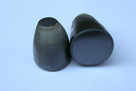
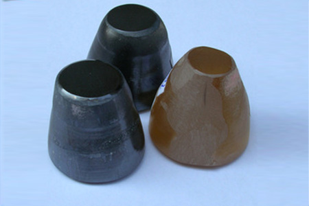
The process begins with growing the sapphire crystal.The most common method for growing sapphire crystals is the Kyropoulos (KY) method or the Czochralski (CZ) method, where a sapphire seed crystal is dipped into molten alumina (Al₂O₃), and the crystal is slowly pulled out while it cools to form a large sapphire boule. This step sets the foundation for the wafer's quality and crystal orientation.
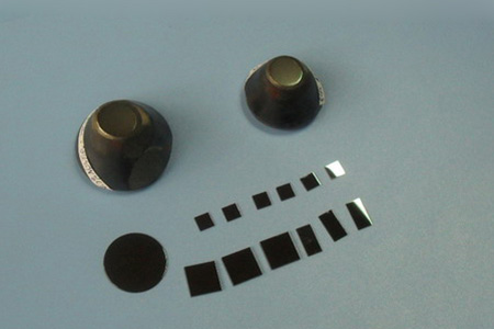
The sapphire boule is precisely oriented in the slicing machine.This step is crucial for ensuring that the slicing machine can make accurate cuts based on the crystal's structure, allowing for uniform thickness and performance in the wafers. Proper alignment ensures that each wafer maintains the desired crystalline orientation for later applications.
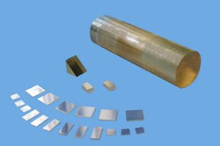
Using a diamond wire saw, the sapphire crystal rod is sliced into thin wafers. The slicing process must be carried out with precision to avoid excessive material loss and minimize surface damage. Each wafer is carefully monitored to maintain consistent thickness across the entire batch.
The wafers undergo grinding to remove the damage layer caused by the slicing process. This step reduces surface damage from slicing and ensures that the wafer's thickness is even across its entire surface. It is essential for further processing and achieving high-performance results in end-use applications.
The edges of the wafer are trimmed and rounded through chamfering. By creating a smooth, rounded edge, this step improves the mechanical strength of the wafer and helps prevent stress concentration, which could otherwise lead to cracks or chips during handling and use.
Polishing refines the surface of the wafer, reducing its roughness and improving its smoothness. This process is performed using specialized chemical mechanical polishing (CMP) techniques to create a mirror-like surface. The polishing stage is critical to preparing the wafer for epitaxial growth, ensuring it meets precision standards for surface finish.
After polishing, the wafer is meticulously cleaned to remove all contaminants such as dust particles, metal residues, and organic compounds. This cleaning process often involves multiple chemical cleaning steps to ensure the wafer is completely free of any impurities that could interfere with later stages of processing.
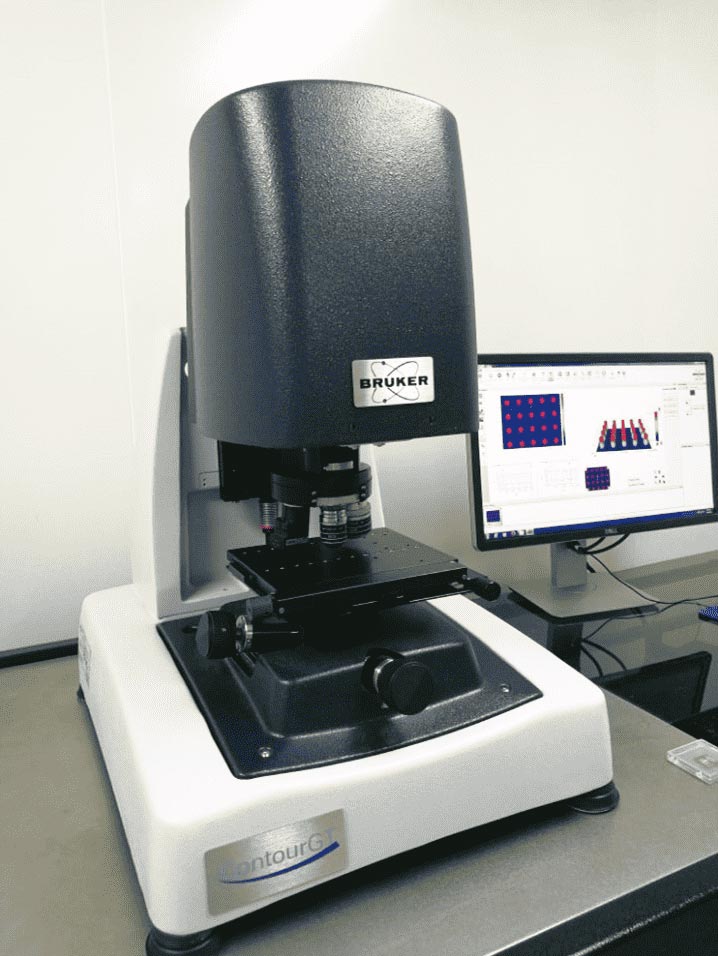
Flatness and thickness are critical factors in sapphire wafer production, especially for high-precision applications like semiconductor manufacturing. Optical interferometers or contact profilometers are commonly used to measure these parameters. Any deviation in flatness or thickness can affect the wafer's performance, leading to alignment issues in downstream processes. Maintaining uniform thickness ensures that the wafers function reliably in demanding environments.
Surface roughness is a key indicator of the polishing quality of sapphire wafers, directly impacting their performance in applications requiring epitaxial layer growth. Tools such as atomic force microscopes (AFM), scanning electron microscopes (SEM), and optical profilometers are used to assess surface roughness. Achieving a smooth surface is crucial, as any imperfections can negatively affect the final product's quality, especially in high-tech industries.
Maintaining a contamination-free surface is essential for the successful application of sapphire wafers. Particle contamination testing is conducted using surface scanners, such as particle counters and wafer inspection tools, to detect any dust, metal particles, or other contaminants. Even microscopic particles can lead to defects or failure in devices, making this test crucial for ensuring cleanliness before further processing stages.
Edge quality is crucial for preventing cracks or damage to sapphire wafers, which can occur due to stress concentration during handling. This step involves high-magnification visual inspection or the use of automated edge inspection systems. Properly chamfered and defect-free edges enhance the wafer's mechanical strength and durability, minimizing the risk of breakage during transport or application.
The crystalline structure of sapphire wafers is essential for their optical and electrical properties. X-ray diffraction (XRD) and Laue back-reflection techniques are commonly used to examine this structure. These tests check for lattice defects, dislocations, and crystal orientation, ensuring that the sapphire wafers meet stringent performance standards, particularly in high-precision applications like LEDs and semiconductors.
Surface defects, such as scratches or pits, can significantly affect the performance of sapphire wafers. Automated inspection systems or manual visual inspections using high-powered microscopes are employed to identify and minimize such defects. Ensuring a defect-free surface is crucial for applications where even small imperfections could compromise the quality of the end product.

Sapphire is one of the hardest materials, second only to diamond on the Mohs scale. This exceptional hardness makes sapphire wafers highly resistant to scratches, mechanical damage, and wear, ensuring long-lasting performance even in harsh environments.

Sapphire has excellent thermal stability, allowing it to withstand high temperatures without degrading. This makes it ideal for applications in high-temperature environments such as semiconductor processing, LEDs, and power electronics.

Sapphire is chemically inert and highly resistant to acids and alkalis, making sapphire wafers ideal for use in chemically aggressive environments. This resistance ensures longevity and reliability in harsh conditions where other materials may degrade.

Sapphire is transparent over a wide wavelength range, from ultraviolet (UV) to infrared (IR). This high optical transparency makes sapphire wafers suitable for optical applications, such as in laser windows, lenses, and optoelectronic devices.

Sapphire is an excellent electrical insulator with low dielectric loss, which makes it useful in electronic devices where electrical isolation is necessary. This feature is particularly valuable in high-frequency and microwave circuits.

In addition to its thermal stability, sapphire also has good thermal conductivity, which helps in dissipating heat efficiently. This is critical in applications like high-power LEDs and RF (radio frequency) devices, where heat management is essential.

Sapphire wafers offer high crystal purity and structural integrity, making them ideal substrates for growing epitaxial layers in semiconductor manufacturing, such as for GaN (gallium nitride)-based devices used in LEDs and power electronics.

Sapphire wafers are highly resistant to radiation, which makes them suitable for use in radiation-rich environments like space applications or in nuclear reactors where materials must withstand intense radiation without performance degradation.

Sapphire wafers serve as substrates for high-frequency radio frequency (RF) and microwave devices. Their excellent electrical insulation and low dielectric loss make them perfect for use in devices that require efficient signal transmission without interference, such as in wireless communication systems, mobile phones, and satellite communication.
The high thermal conductivity and stability of sapphire wafers allow them to be used in high-power electronics, such as power amplifiers and power transistors. They are crucial in power management systems that operate under high voltage and current conditions, especially in industries like automotive, aerospace, and energy.
Sapphire is widely used as a substrate for gallium nitride (GaN) epitaxy in the production of high-performance semiconductors. GaN-based devices are essential for LED lighting, power electronics, and high-frequency RF applications. Sapphire's excellent thermal and structural stability ensures the high-quality growth of GaN layers.
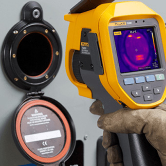
Sapphire's ability to withstand extreme temperatures makes it ideal for use in high-temperature electronic devices, such as sensors, thermocouples, and advanced integrated circuits (ICs) that operate in harsh environments, including industrial and aerospace applications.
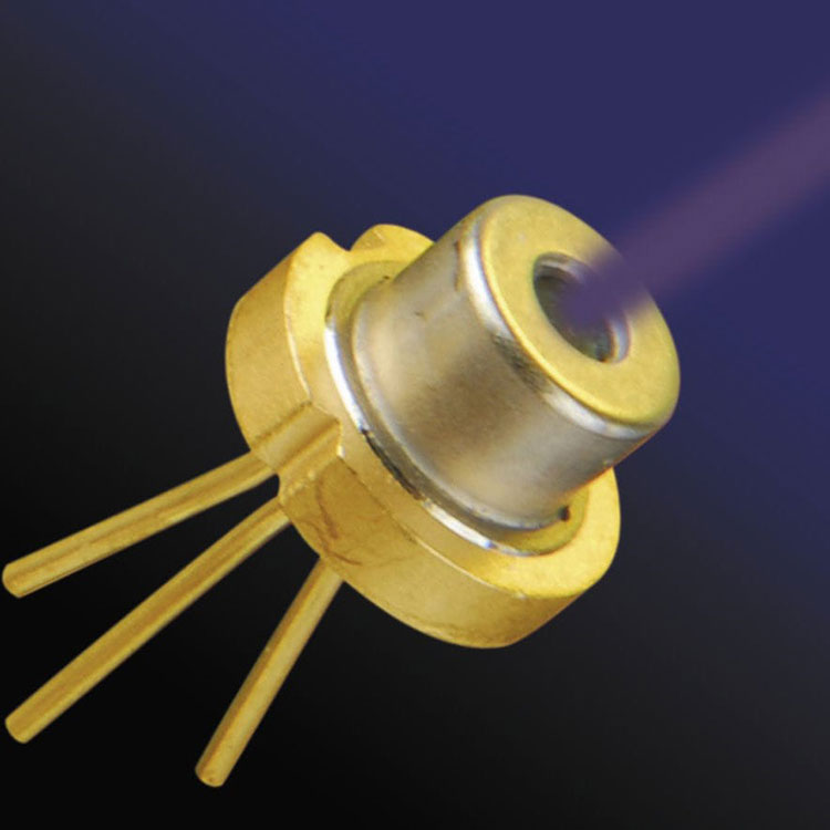
Sapphire wafers are frequently used in optoelectronics due to their transparency over a wide range of wavelengths, from ultraviolet (UV) to infrared (IR). This makes them suitable for optical sensors, laser diodes, and optical communication systems, where clear and precise light transmission is critical.

One of the most common applications of sapphire wafers is in the production of LEDs. Sapphire serves as the substrate for GaN-based LEDs, which are used in displays, lighting, and indicator systems. Its high thermal conductivity helps manage the heat generated by LEDs, improving efficiency and longevity.
Due to its optical clarity and durability, sapphire wafers are used to create infrared and UV windows for various scientific and industrial applications, such as in spectroscopy, medical imaging, and laser systems.
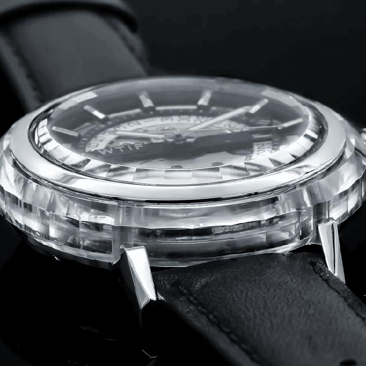
Sapphire's hardness and scratch resistance make it an ideal material for high-end watch crystals and durable windows in harsh environments, such as in aerospace and military-grade equipment.
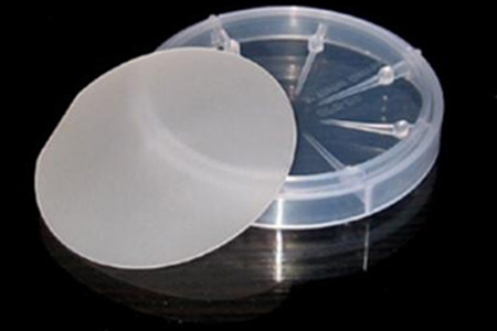
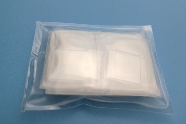
Packaged with class 100 clean bag or wafer container in a class 1000 clean room.
Sapphire wafers are made from single-crystal aluminum oxide (Al₂O₃). This material is known for its exceptional hardness, thermal stability, and optical transparency, making it suitable for various high-tech applications, including semiconductors, optoelectronics, and LED production.
When selecting sapphire wafers for epitaxy, key factors include crystal orientation, surface roughness, and thickness uniformity. These factors directly impact the quality of the epitaxial layer growth, which is critical for applications like LEDs and power electronics.
Yes, sapphire wafers can be customized to meet specific requirements, including size, thickness, crystal orientation, and surface finish. Many manufacturers offer custom solutions to match the unique needs of different industries.
The crystal orientation of sapphire wafers is critical for the performance of epitaxial layers. Different orientations, such as the commonly used c-plane (0001), a-plane (11-20), or r-plane (1-102), are selected based on the specific material growth requirements. For example, the c-plane orientation is widely used in GaN epitaxy for LED and power device applications.
In some applications, sapphire wafers can be reused after careful cleaning and reprocessing. However, their reusability depends on the type of application, the extent of processing, and whether the wafer has sustained any damage or surface contamination. Reusable wafers are more commonly found in research and development settings.
Sapphire and quartz both offer high optical transparency, but sapphire has superior mechanical strength and thermal stability. While quartz is less expensive and easier to process, sapphire's higher durability and scratch resistance make it ideal for applications requiring long-lasting and high-performance materials, such as in high-pressure windows, aerospace, and defense optics.
Sapphire wafers offer environmental benefits due to their durability and longevity. Their ability to withstand extreme conditions reduces the need for frequent replacements, minimizing material waste. Additionally, sapphire is a stable, non-toxic material, which contributes to environmentally friendly manufacturing processes, especially in high-tech industries like electronics and optoelectronics.
After handling, sapphire wafers should undergo a precise cleaning process to remove any contaminants that could affect performance. The cleaning procedure typically includes rinsing with deionized water, ultrasonic cleaning in solvents like acetone or isopropyl alcohol, and drying with filtered nitrogen gas. Proper handling and storage in clean environments can also prevent contamination.
Sapphire wafers should be stored in a clean, dry, and dust-free environment to prevent contamination and surface damage. They are often stored in specialized carriers or containers designed to protect them from physical damage and environmental contaminants. Maintaining a controlled environment with stable temperature and humidity is crucial to ensuring the longevity and quality of the wafers before use.
Please be advised that customised specification sapphire wafers require approximately 3-4 weeks for shipping. If the order is for a regular specification and we have stock, it can be shipped in 1-2 weeks. Please also understand that if transportation volume accumulates during holidays, the delivery time may be slower.
| Superconducting Substrates | |
| Magnetic Ferroelectricity Substrates | |
| Semiconductor Wafers | |
| GaN Thin Film Substrates | |
| Halide Substrates | |
| Ceramic Substrates | |
| Metal Substrates |