Magnesium Oxide Wafer (MgO)
Magnesium Oxide Wafer
Magnesium oxide (MgO) single crystal wafers are widely used in film technology fields, such as the production of magnetic films, semiconductor films, optical films, and high-temperature superconducting films. It is an essential high-temperature superconducting thin film wafer which is currently industrialized. It can be used to fabricate high-temperature superconducting microwave filters and other required devices for mobile communication equipment.
Magnesium Oxide Wafer Physical Properties
| Material | MgO |
|---|---|
| Structure | Cubic |
| Lattice (A) | a=4.130 |
| Growth Method | Special Arc Melting |
| Hardness | 5.5 (Mohns) |
| Purity | 99.95% |
| Crystal Cleavage Plane | <100> |
| Melting Point | 2800℃ |
| Density(g/cm3) | 3.58 g/cm3 |
| Thermal Expansion | 11.2 (x 10-6/℃) |
| Permittivity | ε = 9.65 |
| Optical Transmission | >90%(200~400nm),>98%(500~1000nm) |
Magnesium Oxide Wafer Specifications
| Size | 10x3, 10x5, 10x10, 15x15, 20x20,Dia 2''x 0.33 mm, Dia 2'' x 0.43 mm |
|---|---|
| Thickness | 0.5 mm, 1.0 mm |
| Polished | SSP or DSP |
| Orientation | <001> |
| Redirection Precision | ±0.5° |
| Redirection the Edge | 2°(special in 1°) |
| Angle of Crystalline | Special size and orientation are available on demand. |
| Ra: | ≤5Å(5µm×5µm) |
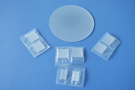
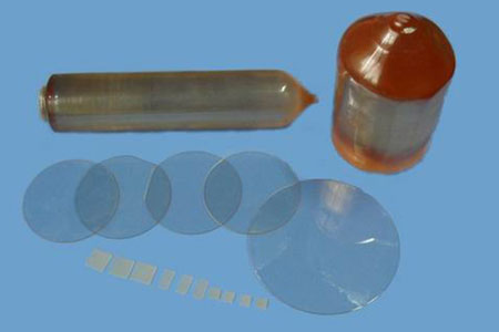
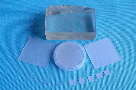
Magnesium Oxide Wafer Package
Packaged with class 100 clean bag or wafer container in a class 1000 clean room.
Related Products of Magnesium Oxide Wafer
|
Magnetic Ferroelectricity Substrates |
Semiconductor Wafers |
|
|
GaN Thin Film Substrates |
Halide Substrates |
Ceramic Substrates |
FREE QUOTE
 Click to download datasheet about Magnesium Oxide Wafer (MgO)
 Unable to find the required data sheet? Click here to send an email and get it.
 Click here to get answers to Frequently Asked Questions (FAQ).