Sputtering Targets
Evaporation Materials
Evaporation Sources
High Purity Materials
Thin Film Substrates
Crytstal Materials


 +86-731-89578196
 [email protected]
Sputtering Targets

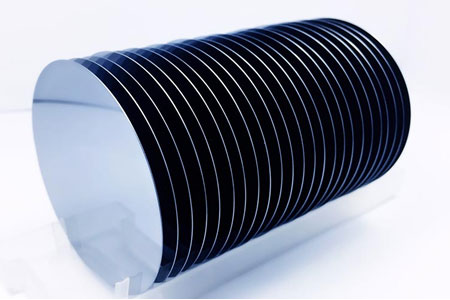
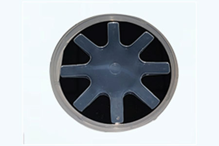
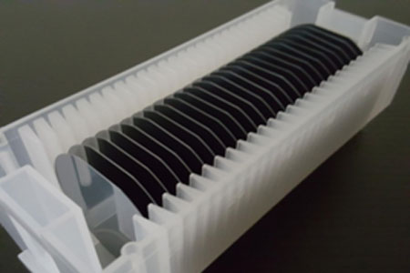
At AEM, we are dedicated to providing high-quality Indium Phosphide wafers, crafted with precision and backed by years of expertise. Our advanced manufacturing and stringent quality controls ensure each wafer delivers top-tier performance and reliability.
Our Indium Phosphide wafers offer key advantages, including excellent thermal stability, high electron mobility, and low defect density. With a focus on quality and precision, AEM's wafers are the perfect solution for advanced technology needs.
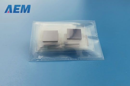
| Size | 10 x 10 x 0.35mm, 10 x 5 x 0.35mm, 2'' Dia, 3'' Dia,4' Dia (customized sizes are available) | |||||
|---|---|---|---|---|---|---|
| Thickness | 0.35 mm, 0.6 mm | |||||
| Polished | SSP or DSP | |||||
| Orientation | <100>, <111> | |||||
| Redirection Precision | ±0.5° | |||||
| Primary Flat Length | 16±2 mm, 22±2 mm, 32.5±2 mm | |||||
| Scondary Flat Length | 8±1 mm, 11±1 mm, 18±1 mm | |||||
| TTV | <10 um, <15 um | |||||
| Bow | <10 um, <15 um | |||||
| Warp | <15 um | |||||
| Material | InP | |||
|---|---|---|---|---|
| Growth Method | LEC,VCZ/P-LEC , VGF, VB | |||
| Lattice (A) | a=5.869 | |||
| Structure | M3 | |||
| Melting Point | 1600℃ | |||
| Density(g/cm3) | 4.79 g/cm³ | |||
| Doped Material | Undoped | S-doped | Zn-doped | Fe-doped |
| Type | N | N | P | N |
| Carrier Concentration (cm-3) | (0.4-2) x 10¹⁶ |
(0.8-3) x 10¹⁸ (4-6) x 10¹⁸ |
(0.6-2) x 10¹⁸ | 10⁷-10⁸ |
| Mobility (cm2v-1s-1) | (3.5-4) x 10³ |
(2.2-2.4) x 10³ (1.3-1.6) x 10³ |
70-90 | ≥2000 |
| EPD (Average) | <5 x 10⁴/cm² |
3 x 10⁴/cm² 2 x 10³/cm² |
2 x 10⁴/cm² | 3 x 10⁴/cm² |
Our wafers are manufactured with strict quality control to ensure low defect density and unmatched purity.
AEM's advanced production techniques guarantee wafers with exceptional precision and consistency.
We offer flexible customization options to meet specific technical requirements and project demands.
With our robust production capabilities, we ensure a consistent and timely supply of high-performance wafers.
With years of experience in wafer manufacturing, AEM is a trusted leader in the industry.
The process starts with selecting high-purity indium and phosphorus, along with hydrogen gas. These raw materials are carefully prepared and handled in a cleanroom environment to ensure purity and stability, preventing contamination during subsequent steps.
The phosphidation reaction takes place in specialized equipment like a rotary furnace or vapor deposition reactor, which operates at high temperatures and pressures. The reactor's design considers factors such as corrosion resistance, heating precision, and airtight sealing to ensure a controlled reaction environment.
Indium and phosphorus are introduced into the reaction chamber under controlled temperature and pressure. Hydrogen gas is added to regulate the reaction speed. These elements react to form Indium Phosphide (InP) in bulk crystal form. After the reaction, cooling is applied, and gases are safely vented.
After the phosphidation reaction, the InP crystal is grown using techniques like the Vertical Gradient Freeze (VGF) or Czochralski process. A seed crystal is slowly pulled from a melt of indium and phosphorus, allowing the InP crystal to form layer by layer, creating a large single-crystal ingot.
The InP crystal undergoes annealing, a process in which the crystal is slowly heated and cooled to relieve internal stresses. This enhances the crystal's structural integrity, reducing defects and improving its overall quality.
The annealed InP crystal is sliced into thin wafers using precision cutting tools like diamond wire saws. This slicing process ensures uniform thickness and prepares the wafers for further processing.
After slicing, the wafers are lapped to remove saw marks and roughness from the surface. They are then polished to achieve a smooth, mirror-like finish. Polishing ensures the wafer surface is defect-free and ready for subsequent applications.
Next, the wafers undergo chemical etching to remove surface damage caused by slicing and polishing. They are then cleaned with ultra-pure water and chemicals to eliminate any remaining particles or contaminants, ensuring a pristine surface.

InP wafers exhibit exceptional electron mobility, which allows for faster electron movement through the material. This makes InP ideal for high-frequency and high-speed electronic devices such as high-performance transistors, high-speed communication systems, and millimeter-wave applications.

InP has a direct bandgap, making it highly efficient for emitting light, which is essential for optoelectronic applications like lasers, light-emitting diodes (LEDs), and photodetectors. Its direct bandgap allows for efficient photon generation and absorption in devices such as optical transceivers and fiber-optic communications.

The combination of high electron mobility and low resistance to electron flow allows InP devices to exhibit low noise levels and high power efficiency. This is particularly advantageous in microwave and high-frequency power amplifiers, where signal clarity and strength are crucial.

InP has better thermal conductivity compared to many other semiconductor materials. This allows it to effectively dissipate heat generated during high-power or high-frequency operations, making it suitable for high-performance devices where heat management is critical.

InP wafers have a high breakdown voltage, meaning they can withstand higher electric fields before experiencing electrical breakdown. This makes them highly reliable in power devices and high-voltage applications, where they can operate safely at higher voltages.

InP has good resistance to radiation, making it well-suited for use in satellite communication systems and space applications, where materials are exposed to high levels of radiation.

InP wafers generally exhibit low defect densities, particularly when grown using advanced techniques like the Vertical Gradient Freeze (VGF) method. This ensures higher performance and reliability in electronic and optoelectronic devices.

InP is highly transparent to infrared light, making it an excellent material for photonic devices, infrared detectors, and fiber-optic communication systems that operate in the infrared spectrum.

Indium Phosphide wafers play a key role in optoelectronic terahertz technology used in the automotive sector. They are crucial in ultra-sensitive spectroscopic analyzers and polymer thickness measurements. InP-based technology helps detect multilayer coatings and improves precision in automotive manufacturing, enabling better quality control and material assessment.
InP wafers are integral to high-speed microelectronics. They enable the development of cutting-edge devices such as High Electron Mobility Transistors (HEMT) and heterostructure bipolar transistors, making them the fastest semiconductors available. Their high electron mobility ensures excellent performance in high-frequency electronics like millimeter-wave and communication systems.
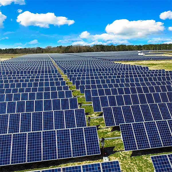
Indium Phosphide wafers are used in the most efficient photovoltaic cells, achieving up to 46% efficiency. InP substrates are essential for producing low-bandgap materials required for high-quality crystalline solar cells. This makes InP a vital component in advanced solar energy systems, improving energy conversion and reducing power loss.
InP is utilized in photonic integrated circuits (PICs), enabling laser generation, amplification, control, and detection within a single chip. This makes it ideal for optical communication and sensing applications, where high-speed data transmission and signal integrity are critical.

In the medical field, InP wafers are used in optoelectronic devices for surgery equipment control and vital sign monitoring systems. Their high precision and performance in detecting and controlling medical processes make them invaluable in healthcare technologies.
Indium Phosphide wafers are employed in hybrid silicon lasers, offering an alternative to traditional silicon. This breakthrough in photonics allows for more efficient and cost-effective production of laser-integrated circuits, reducing expenses and improving performance in communication systems.
InP wafers are used in InP-based heterojunction bipolar transistors, which offer high electron mobility and saturation velocity, making them perfect for optical fiber transmission windows. They are also essential in producing lasers, photodetectors, and other optoelectronic devices used in telecommunications.
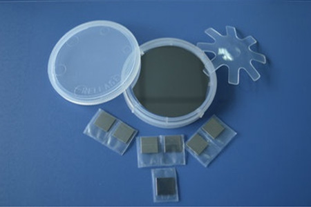
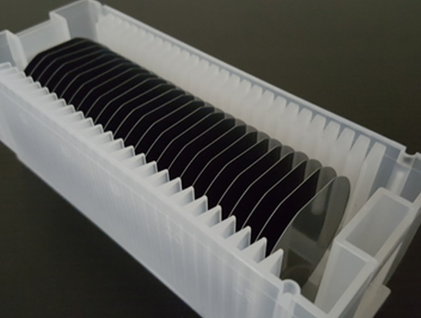
Packaged with class 100 clean bag or wafer container in a class 1000 clean room.
An Indium Phosphide (InP) wafer is a semiconductor material made from a combination of indium and phosphorus, commonly used in high-frequency electronics and optoelectronics.
Indium Phosphide is a direct bandgap material, meaning it can efficiently emit light, which is beneficial for optoelectronic devices.
Producing large-diameter InP wafers is challenging due to the difficulty in maintaining crystal uniformity and reducing defect density over larger areas.
Surface passivation of InP wafers can be achieved through the deposition of dielectric materials like silicon nitride or oxides to protect the surface and improve device performance.
Like most semiconductors, the performance of InP devices degrades at high temperatures, but its superior thermal properties make it more resilient than many alternatives.
InP wafers serve as a substrate for epitaxial growth, allowing layers of other materials like InGaAs or AlInAs to be deposited for device fabrication.
InP wafers can be reclaimed and reused after re-polishing, though the process is more complex compared to silicon wafer recycling.
Yes, phosphorus compounds can be toxic, so proper handling procedures, including ventilation and protective equipment, are required during production.
InP wafers should be stored in clean, dry, and controlled environments to avoid contamination or degradation over time.
Please be advised that customised specification InP wafers require approximately 3-4 weeks for shipping. If the order is for a regular specification and we have stock, it can be shipped in 1-2 weeks. Please also understand that if transportation volume accumulates during holidays, the delivery time may be slower.
| Superconducting Substrates | |
| Magnetic Ferroelectricity Substrates | |
| Semiconductor Wafers | |
| GaN Thin Film Substrates | |
| Halide Substrates | |
| Ceramic Substrates | |
| Metal Substrates |